
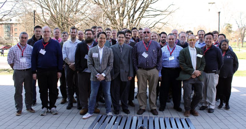
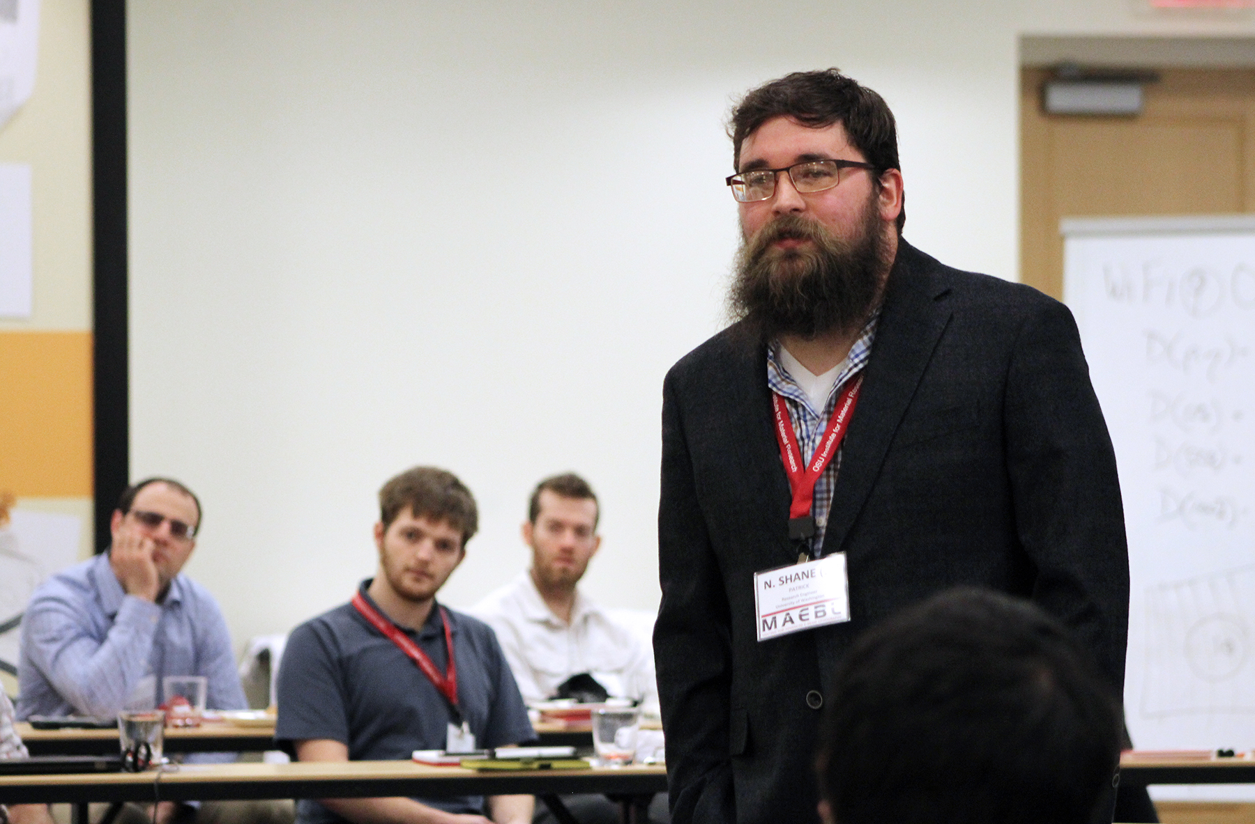
The Ohio State University in April hosted dozens of expert and novice users of electron beam lithography tools from across the country at the third annual Meeting for Advanced Electron Beam Lithography (MAEBL) at the Ohio Union.
The workshop connects users with varying levels of experience with e-beam lithography tools, offering an open format to exchange knowledge. The MAEBL community is comprised of engineers, scientists and students from industry, academia, and government that use e-beam lithography to enable cutting-edge research and development.
E-beam lithography, or EBL, is the process of focusing an electron beam onto a film covered in electron-sensitive material. This alters the solubility of the film and, ultimately, allows a precise nanostructure to be patterned in the surface before being transferred to a substrate.
Speakers at MAEBL this year came from Ohio State, University of Delaware, University of Pennsylvania, California Institute of Technology, Massachusetts Institute of Technology, Yale University, University of Washington, and Sandia National Lab.

Aimee Price, senior research associate at Nanotech West Laboratory, worked to bring this year’s workshop to Ohio State with fellow steering committee members Kevin Lister, lithography engineer at the University of Delaware Nanofabrication Facility, and Gerald Lopez, director of business development at the University of Pennsylvania Singh Center for Nanotechnology.
“Ohio State has extensive EBL expertise and is the major EBL hub in the state of Ohio, serving both internal OSU researchers and external institutions throughout the country,” Price said. “Hosting MAEBL at Ohio State was an incredible opportunity to bring the EBL community to the Midwest. Although there are several EBL installations within driving distance, the Midwest is often overlooked due to the large concentration of systems on the East and West Coasts. Additionally, IMR has remarkable technical event planning capability which ensured a smooth, well-run meeting. I can’t thank Angie Dockery, Ciara Donovan, and the Ohio Union staff enough. They ensured that the meeting details were impeccable, so the steering committee members could focus on the technical talks.”
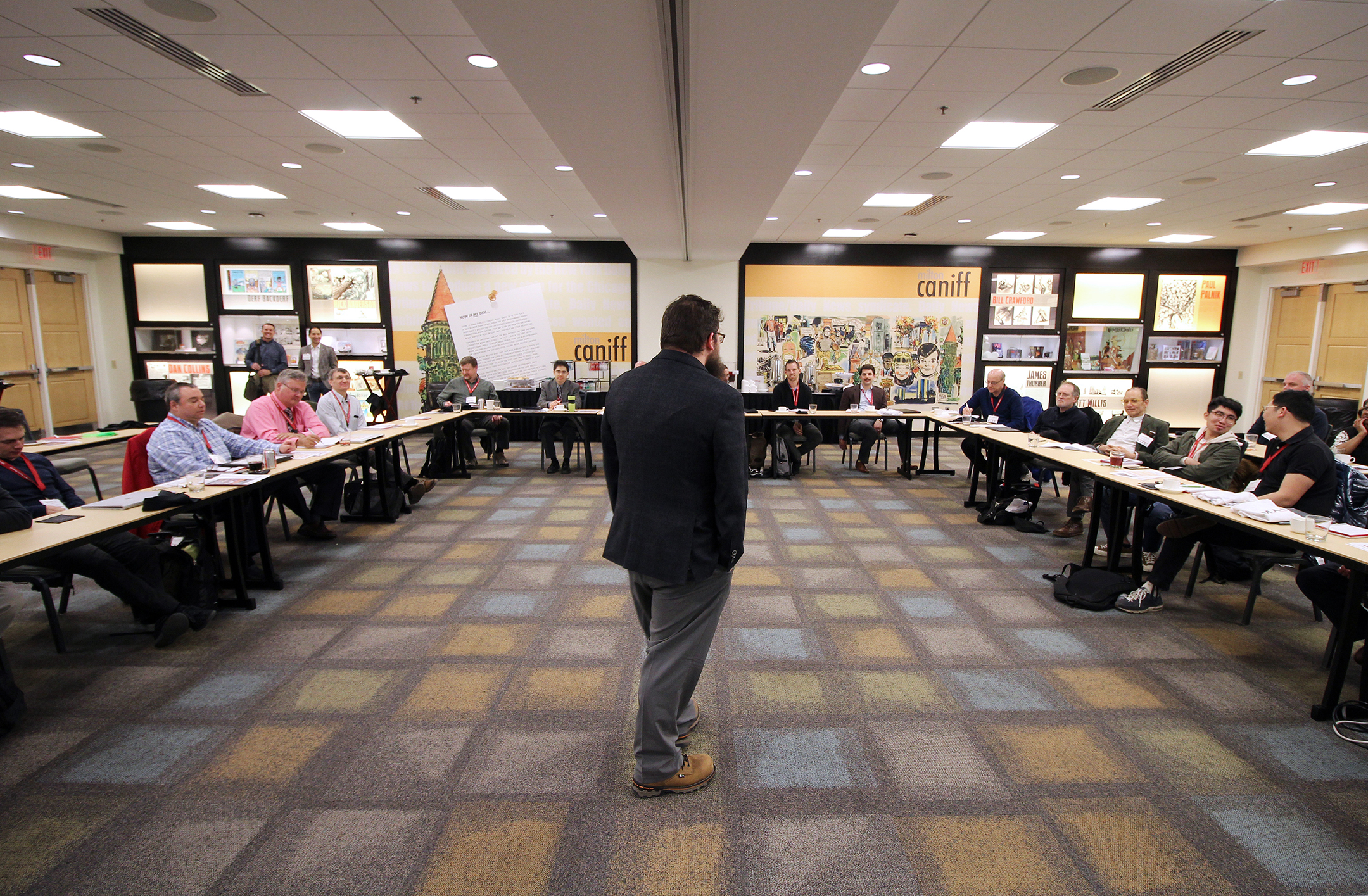
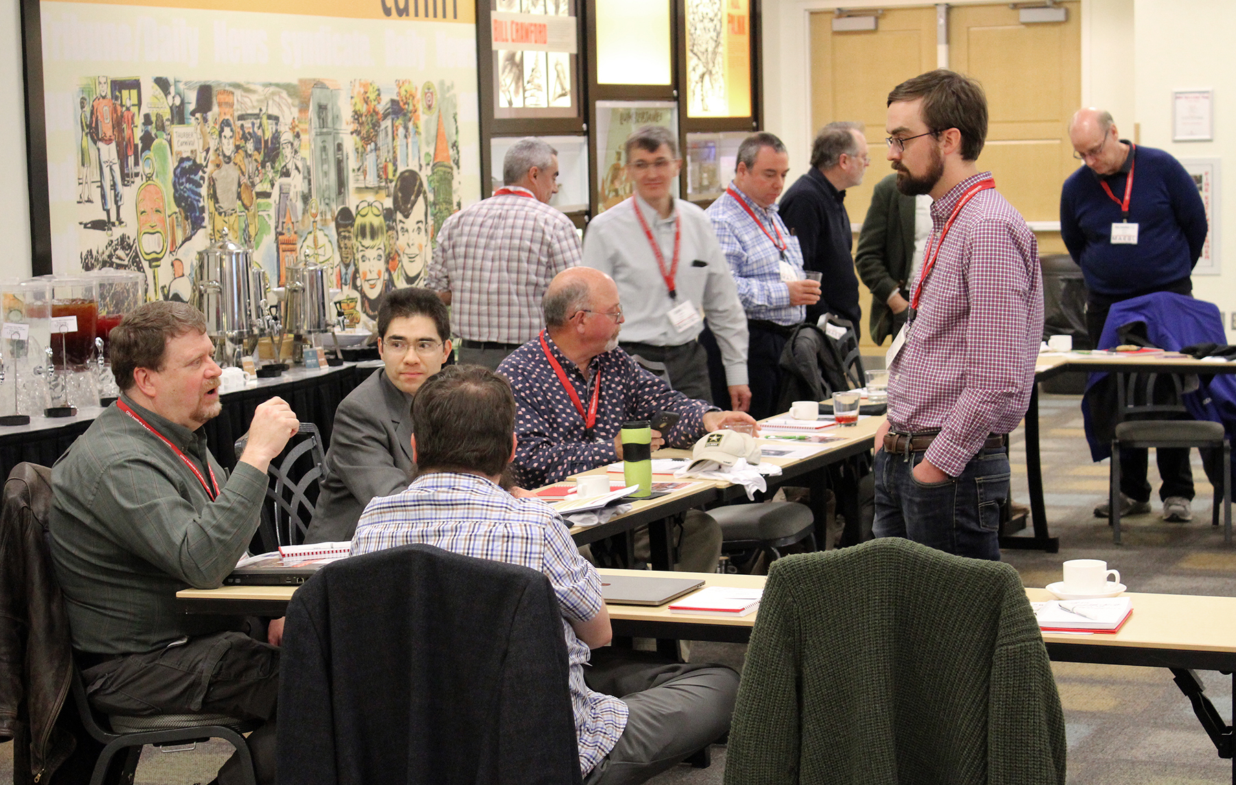
The event allowed attendees from the often-segmented e-beam lithography community to come together for a dialogue about the state-of-the-art systems in a uniquely intimate, informal space.
“The EBL community is small, yet geographically scattered and growing,” Lopez said. “At our conferences, there are too many familiar faces who don’t know each other unless they share a similar brand of tool. If we did find ourselves in the same room, there was always someone else running the show. What makes us different is that we’re not a conference where something “new” has to be discussed. We’re a workshop, a place to exchange ideas — new and old — and more strategically, a networking platform. MAEBL gives the EBL community a voice — a chance to finally connect and learn from one another. So far it’s been well received so much so that the vendors have chartered sponsorship for the first time.”

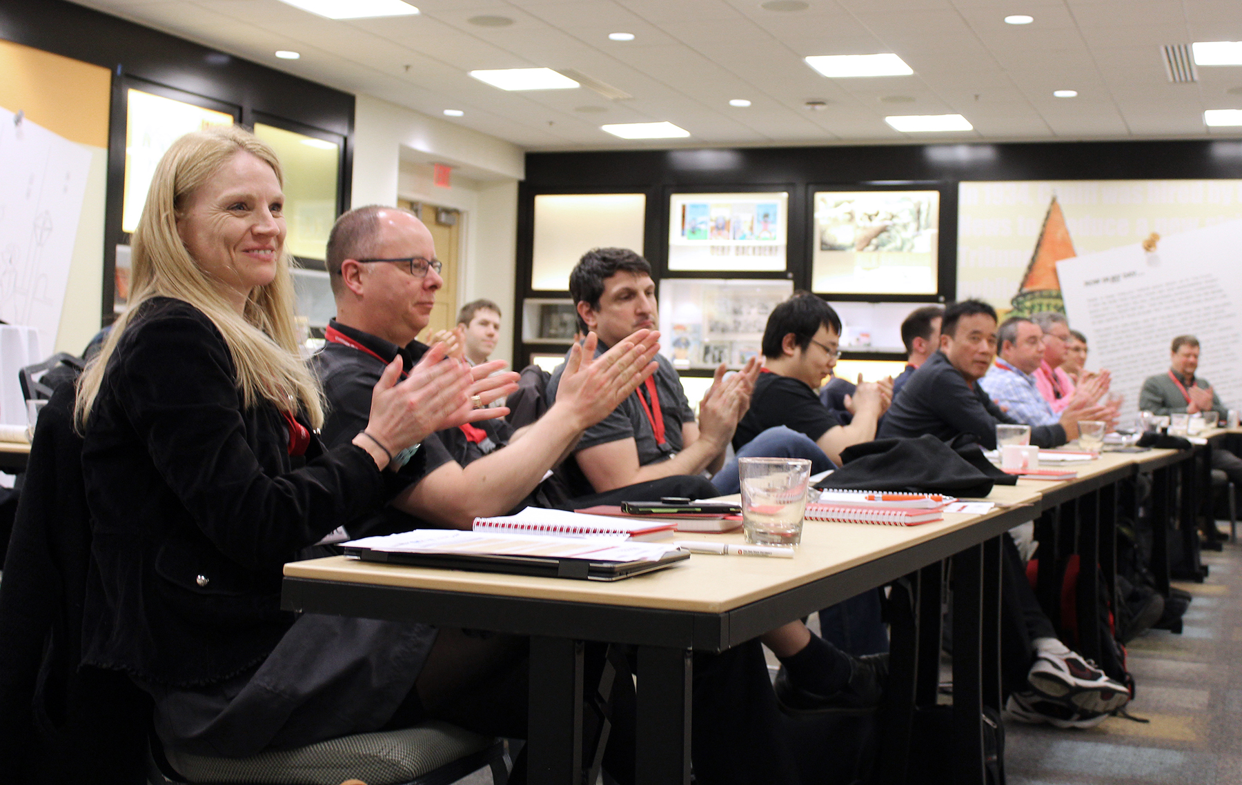
The one-day event was chock-full of networking opportunities and talks ranging from data preparation to device fabrication, with several group discussions to identify common challenges in the community. Additionally, on the day before the MAEBL meeting, IMR and the Nanotech West Lab hosted a seminar, presented by Dr. Gerald Lopez, for beginner EBL operators and researchers, covering the basics of EBL pattern generation. The seminar has become the pilot study for a second day of MAEBL in future meetings, which will focus on basic education in the field. This will better serve the new members of the community, while continuing to add value to the advanced users.
This year’s MAEBL was supported through its charter sponsors: JEOL USA, Raith Nanofabrication, STS-Elionix, AllResist and LatticeGear.
Ohio State’s e-beam lithography capability at the Nanotech West Lab features a Leica/Vistec EBPG 5000 field-emission electron beam pattern generator (EBL01). The tool can operate at 50 and 100 keV, using beam sizes as small as approximately 5nm, which results in linewidths down to about 20nm. The lab houses CAD layout and data fracturing capability and can accept GDSII, Tanner Database and CTEXT formats, among others.
Article by Mike Huson, IMR Public Relations Coordinator
Contact: huson.4@osu.edu
Follow: @OhioStateIMR