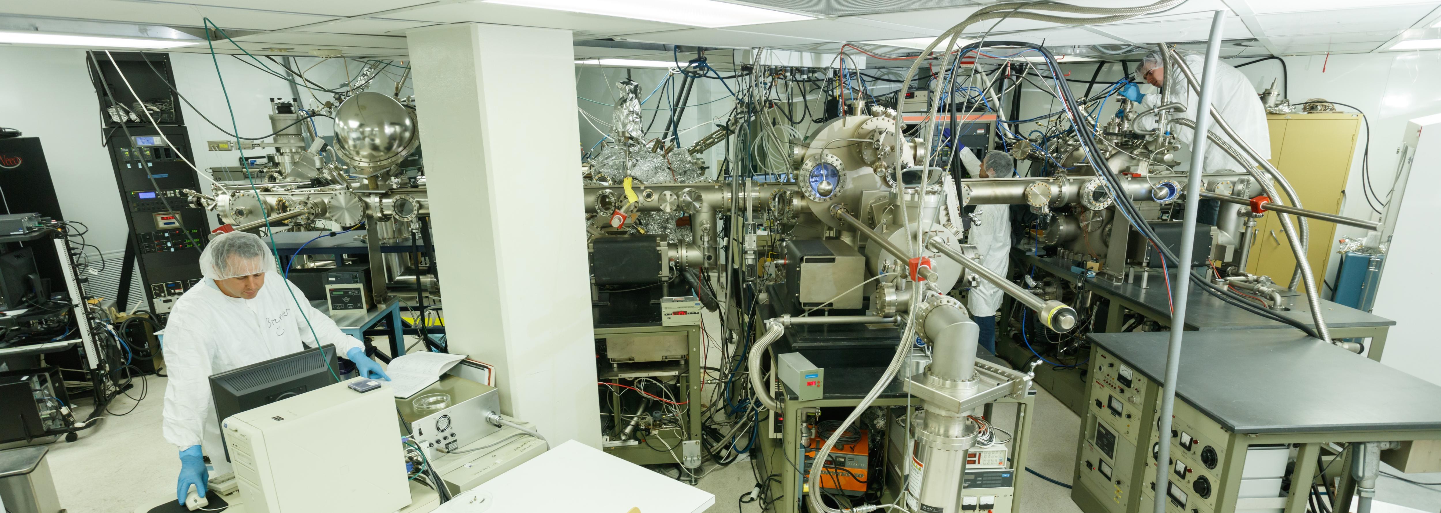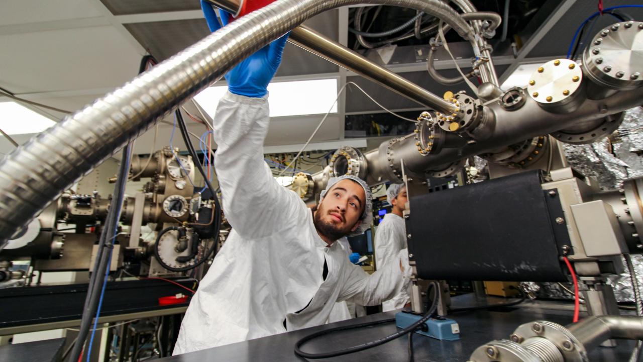
The Semiconductor Epitaxy and Analysis Laboratory (SEAL) is Ohio State’s primary facility for molecular beam epitaxy (MBE). As one of the largest MBE facilities in the U.S., this world-class, shared user facility supports interdisciplinary research and development on epitaxial growth of electronic and photonic materials and devices. SEAL is fully staffed and open to university and industry researchers. SEAL houses six state of the art MBE chambers each dedicated to different, complementary material systems to provide epitaxial growth of crystalline layers, heterostructures, nanostructures and device structures in a variety of material domains.
Research focuses on a range of semiconductor materials, including III-V materials based on arsenides, phosphides, antimonides, nitrides, and advanced oxides, SiGe and 2D materials. SEAL is managed by IMR and operates under the guidance of the Department of Electrical and Computer Engineering and College of Engineering. Several chambers are integrated into UHV cluster tools, enabling a range of hybrid structures and devices. Vacuum Cluster I encompasses two MBE chambers and an analytical system allowing III-V/ IV integration studies and high-resolution X-ray photoelectron spectroscopy for in-situ chemical studies of pristine surfaces and interfaces. Cluster II comprises nitride- and oxide-MBE chambers, the combination of which also enables unique combinations of materials. SEAL has a range of advanced materials characterization tools to support breakthrough epitaxy and electronic materials.