Microelectronics Innovation and Technology Cluster (MITEC)
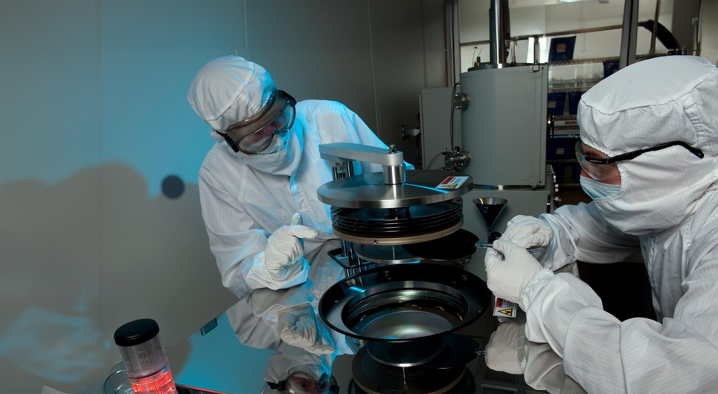
In partnership with the Midwest Microelectronics Consortium (MMEC) and support from the Ohio Department of Higher Education, The Ohio State University launched MITEC, a core facility designed to accelerate U.S. leadership in advanced semiconductor research and development. It integrates new epitaxial growth, device fabrication, and device characterization capabilities into a connected lab-to-fab pipeline for microelectronics research and development.


These capabilities form a lab-to-fab pipeline, enabling prototype devices to be grown, fabricated, and tested on up to 100 mm wafers before transitioning to industry for advancing to higher technology and manufacturing readiness levels. MITEC also connects with OSU’s other research facilities, providing members with an integrated set of tools for advancing microelectronics across a broad range of technologies and material systems.
MITEC creates an integrated semiconductor development path that connects epitaxial materials growth, nanofabrication, and device characterization within Ohio State’s research facility ecosystem. This structure strengthens Ohio State’s ability to support microelectronics research across material systems and device classes, including wide- and ultra-wide-bandgap power devices, RF/microwave devices, infrared optoelectronics, and emerging semiconductor technologies.