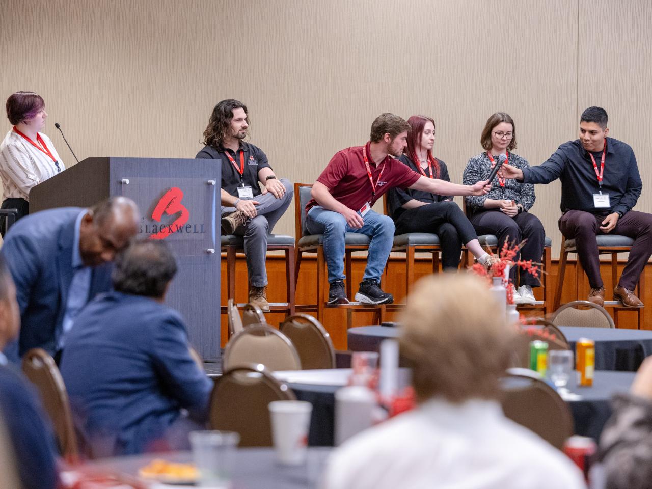
Sanjay Krishna, professor at The Ohio State University:
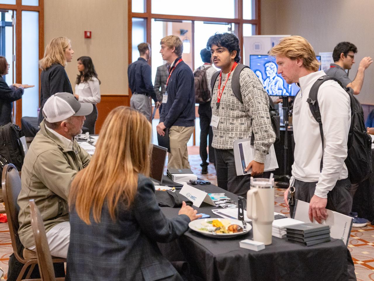
MIST is the mid-infrared semiconductor technology workshop. It's co-hosted by Ohio State and MMEC, which is the Midwest Microelectronics Consortium. We have a critical shortage of semiconductor engineers in this area, and Ohio State has some of the best talent that we can tap into. So the goal of hosting this inaugural workshop is to bring these students together to interact with some of the thought leaders in our field.
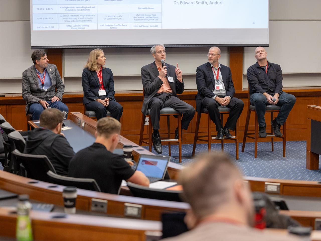
Matt Casto, chief technology officer at the Midwest Microelectronics Consortium:
MMEC, Ohio State and really all of our members within the MMEC ecosystem that are delivering and developing capability for electro-optics and infrared technology — a technology that's extremely critical for our war fighters, for our nation, but also has some really you know critical impacts for our economic development for the state, the region and the nation — so many applications, so many technologies utilize the capabilities, but a very important set of expertise, infrastructure and tools need to be leveraged to actually deliver things on the scale and at the time frames that that are going to be impactful.
Jeremy Goodenough, undergraduate student at the University of Central Florida:
I was not very familiar with how in-depth the world of semiconductor and infrared sensing was. I know a lot of the baseline applications, whether that be for defense imaging or astronomy. I didn't realize how involved all of the systems were that go into creating new and like iterating on those systems, and how widespread it is through academia, national labs and industry.
Elizabeth Steenbergen, senior principal systems engineer at Raytheon:
This is a very unique opportunity, a workshop that wasn't available for us when we were undergrads and, personally, I didn't even know what research was when I was in undergrad. So I went to industry, worked for a few years until I figured out what my passion was, went back to grad school and have had an awesome career thus far. So I think it's really invaluable to undergrads to be exposed to professionals right now who've been through graduate research and graduate students and professors from universities across the nation.
Dhiya Srikanth, undergraduate research assistant at Penn State University:
The conference is a lot different than I expected but, like, better. I love the topics, like some of the things you would need to start your own company. The graduates panel was so informative — and the fellowships — the fellowships was especially great because I'm a senior applying for my grad programs.
Jacob Tenorio, graduate fellow at The Ohio State University:
I think it did a really good job at opening up my eyes to which path I do want to take, and I believe I got my answer just by talking to a lot of the representatives that were here from the either private sector or government as well.
Sanjay Krishna, professor at The Ohio State University:
Ohio State is very strong in compound semiconductors. In particular, we have a very unique capability for atoms to arrays which is the theme of the MIST workshop.
Steven Ringel, professor and IMR executive director at The Ohio State University:
At Ohio State, we're extremely fortunate to have amazing infrastructure where we can create state-of-the-art materials and semiconductors all the way through devices and circuits and systems in one university. It's extremely rare to be able to have such vertical integration capabilities. We have this all across campus in our core departments, like Electrical and Computer Engineering, College of Engineering, our Institute for Materials and Manufacturing Research, where we actually have quite a bit of interaction with corporate partners, government partners — all working with our faculty, our research scientists, our graduate students, our undergraduate students — the entire gamut.
Sanjay Krishna, professor at The Ohio State University:
These have applications ranging from military but all the way to dual application, dual usage technology. For example, everything from medical to greenhouse gas detection to aerospace and engineering. The goal is to have our students trained in these advanced R&D and Ohio State be the seed for providing this capability here.