
 Dr. Leonard Brillson joined The Ohio State University in 1996 as Professor of Electrical & Computer Engineering and Physics, and a Center for Materials Research Scholar. He received his A.B. in Physics at Princeton University in 1967 and his Ph.D. in Solid State Physics at the University of Pennsylvania in 1972.Prior to academia, he held a number of management positions at Xerox Corporation’s Joseph C. Wilson Center for Research and Technology, including directing the Materials Research Laboratory, one of several major research departments in Xerox’s Corporate Research Division. He is an IEEE, APS, AVS, and AAAS Fellow. He has served on several journal boards of editors and the American Institute of Physics Governing Board. He has over 300 peer-reviewed journal articles, invited reviews, monographs and books with over 6,000 citations and an interdisciplinary textbook, “Surfaces and Interfaces of Electronic Materials.” (Wiley, 2010). He holds 2 patents. He has received Ohio State’s Lumley Research Award, Xerox Corporation’s Outstanding Achievement Award, Surface Science Magazine’s Excellence Award, the 2006 AVS Gaede-Langmuir Award, Citation Classic recognition by the Institute for Scientific Information, and 2007 induction into the Phi Kappa Phi National Honor Society.
Research in Dr. Brillson’s laboratory focuses on properties of advanced electronic material thin films and interfaces centered on semiconductors, single crystal complex oxides, and polycrystalline photovoltaics at the nanoscale. Current research emphasizes the electronic and chemical structure of state-of-the-art ferroelectrics, ferromagnets, and multiferroics in combination with wide gap semiconductors, especially the influence of local compositional structure and defects on electromagnetic properties, Schottky barrier formation, and heterojunction band offsets. A renaissance has occurred in the crystalline growth of these electronic materials, and they are having a major impact on environmentally-friendly energy creation, next generation solid state lighting, ultrahigh speed communication, and computing. A new initiative in bioelectronic materials and interfaces aims to produce compact, mass-producible sensors for use in sensitive immunological and pathogen detection. Prof. Brillson’s group makes use of a wide range of ultrahigh vacuum surface and interface science research facilities, including quantum-scale, UHV low energy electron-excited nanoscale luminescence, Auger electron, and secondary ion mass spectroscopies, electron microscopy, molecular beam epitaxy growth facilities, as well as clean room facilities for nanostructure fabrication and processing. This group also has strong interdisciplinary interactions with an extensive electronic materials community on campus.
Research Highlights
Revealing the missing atom that controls ZnO devices
ZnO is a leading semiconductor for next generation optoelectronics. Yet, despite thousands of ZnO papers published each year, the physical nature of defects that dominate its optical spectra and transport properties have remained unresolved. The assignment of these visible emissions to specific Zn/O vacancies, interstitials, or their complexes has been under debate for over 40 years. The particular work described here clearly identifies the physical nature of the defects dominating optical features of this widely studied semiconductor by combining two powerful techniques, positron annihilation spectroscopy (PAS) and depth resolved cathodoluminescence spectroscopy (DRCLS). Indeed, the assignment of these defects provide a consistent explanation for ZnO’s effective free carrier densities on a local scale based on scanning spreading resistance microscopy (SSRM). Previously, we showed that these are the very defects created at the microscopic metal-ZnO junction and that control the movement of electric charge inside the semiconductor. These in turn determine our ability to develop optoelectronics devices such as p-n junctions and laser diodes.
We have now identified the optical emission associated with Zn vacancies using positron annihilation spectroscopy (PAS) coupled with depth-resolved cathodoluminescence spectroscopy (DRCLS). Both techniques are capable of detecting native point defects vs. depth into semiconductors – PAS via changes in positron lifetime with incident positron energy and DRCLS via intensity changes in spectrally-resolved emissions with incident electron energy. In Figure 1(left), DRCLS incident electrons generate an electron cascade (blue), resulting in electron-hole pair generation, recombination, and characteristic defect photon emission (h?). PAS incident positrons scatter and thermalize (orange), recombining with electrons and emitting 2 ? rays time-delayed (?t) by Zn vacancies.
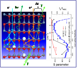
Figure 1
Figure 1: (left) DRCLS and PAS excitation processes, (right) matching depth profiles. Y.Dong et al., Phys. Rev. B 81, 081201(R) (2010).
Figure 1(right) shows the matching PAS and DRCLS defect densities versus Li-implanted ZnO depth. PAS revealed a peak in Zn vacancies 1 micron below the free surface of Li-implanted ZnO, matching an intensity maximum in DRCLS emission of a 2.0 electron volt spectral peak at that depth. Since Zn and O vacancies have opposite charge., we can now understand how these two in combination influence transport in ZnO electronic devices. The light from the Zn vacancy in turn provides a tool for creating p-type ZnO, where positive carriers (“holes”) dominate to enable solid state lasers.
How does your garden (of nanorods) grow?
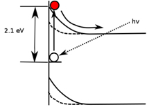
Figure 2. Photoexcitation of an electron from a trap level into the conduction band, decreasing the surface band bending.
Not only is ZnO useful for next generation electronics, but it can also enable these devices on a nanometer scale. ZnO can form beautiful rods, ribbons, and belts from which lasers and transistors can be made with dimensions 10,000 times smaller than a human hair. How these nanostructures grow is the subject of much research activity. We have recently developed an optical technique to measure their electronic properties called nanoscale-resolved surface photovoltage spectroscopy (SPS). SPS involves shining monochromatic light of increasing photon energy h? on the ZnO and measuring with an atomic force microscope the minimum energies needed to populate or depopulate electrical charge traps near the surface. Figure 2 illustrates the photoexcitation of an electron to the conduction band level and its subsequent movement away from the surface. As the charge on the surface changes with photoexcitation, its electric potential changes as well, revealing the trap state energy within the semiconductor band gap.
From DRCLS measurements, we can identify this transition with Zn vacancies, and by probing near the ZnO nanostructures, we discover that ZnO nanorods can create these Zn vacancies spontaneously. Figure 3 illustrates a 20 nm high nanorod or “nanobump”. The Dots mark locations where the SPS spectra were measured. Besides the ZnO band gap peak at 3.4 eV, the pronounced change in slope at ~ 2.1 eV indicates the presence of Zn vacancies below the ZnO surface. With increasing distance from the nanorod, this feature diminishes. This nanorod appeared spontaneously on the otherwise flat ZnO surface after several months of air exposure. We interpret this effect as Zn oxidation of the surface in which Zn atoms combine with air molecules of oxygen to grow new ZnO at the surface. The increasing Zn vacancy concentration near the nanorod reveals that this oxidation process grows ZnO nanorods by gathering Zn from the near-surface region, leaving Zn vacancies behind in the ZnO lattice. This phenomenon reveals not only the nature of the nanostructure growth but also an avenue to control ZnO’s conductivity on a nanoscale.
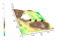
Figure 3. Nanorod and nearby SPS probe sites.
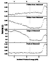
Figure 4. SPS curves showing 2.1 eV Zn vacancy depopulation feature decreasing away from nanorod.
For more information on Dr. Brillson’s or his research please visit his website: http://www.ece.osu.edu/~brillson/