
Each year, the Institute for Materials and Manufacturing Research Distinguished Lecture Series brings world renowned materials researchers to The Ohio State University campus to share the latest developments in materials-allied fields and discuss their research with Ohio State students, faculty and staff. IMR Distinguished Lecturers include the top scientists in their fields.
All IMR Distinguished Lecturers presentations are free and open to the entire Ohio State materials community – faculty, staff and students.
Deep Tech for Human and Planetary Health: Startups Reinventing the Means of Manufacturing
What role can materials and manufacturing play in radically improving human and planetary health? Join us April 16 for an interactive panel investigating the intersection of research, investment, and innovation for societal impact. Preceding the discussion, SOSV founder Sean O’Sullivan will deliver the talk “Deep Tech for Human and Planetary Health.” O’Sullivan’s first startup, MapInfo, popularized computer street mapping, he’s a principal donor to Khan Academy and is credited as co-creating the term “cloud computing.”
Panel and Interactive Discussion:
Panel Moderator: Kieran Drain (Managing Director Entrepreneur in Residence Group, Applied Materials, Inc.)
Panelists: Sean O’Sullivan, Duncan Turner (General Partner at SOSV and the Global Managing Director of HAX), Susan Schofer (Partner at SOSV and Chief Science Officer at HAX)
Click Here to Register
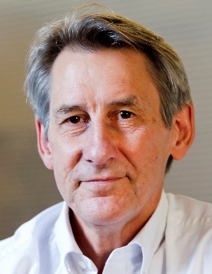
Sean O’Sullivan
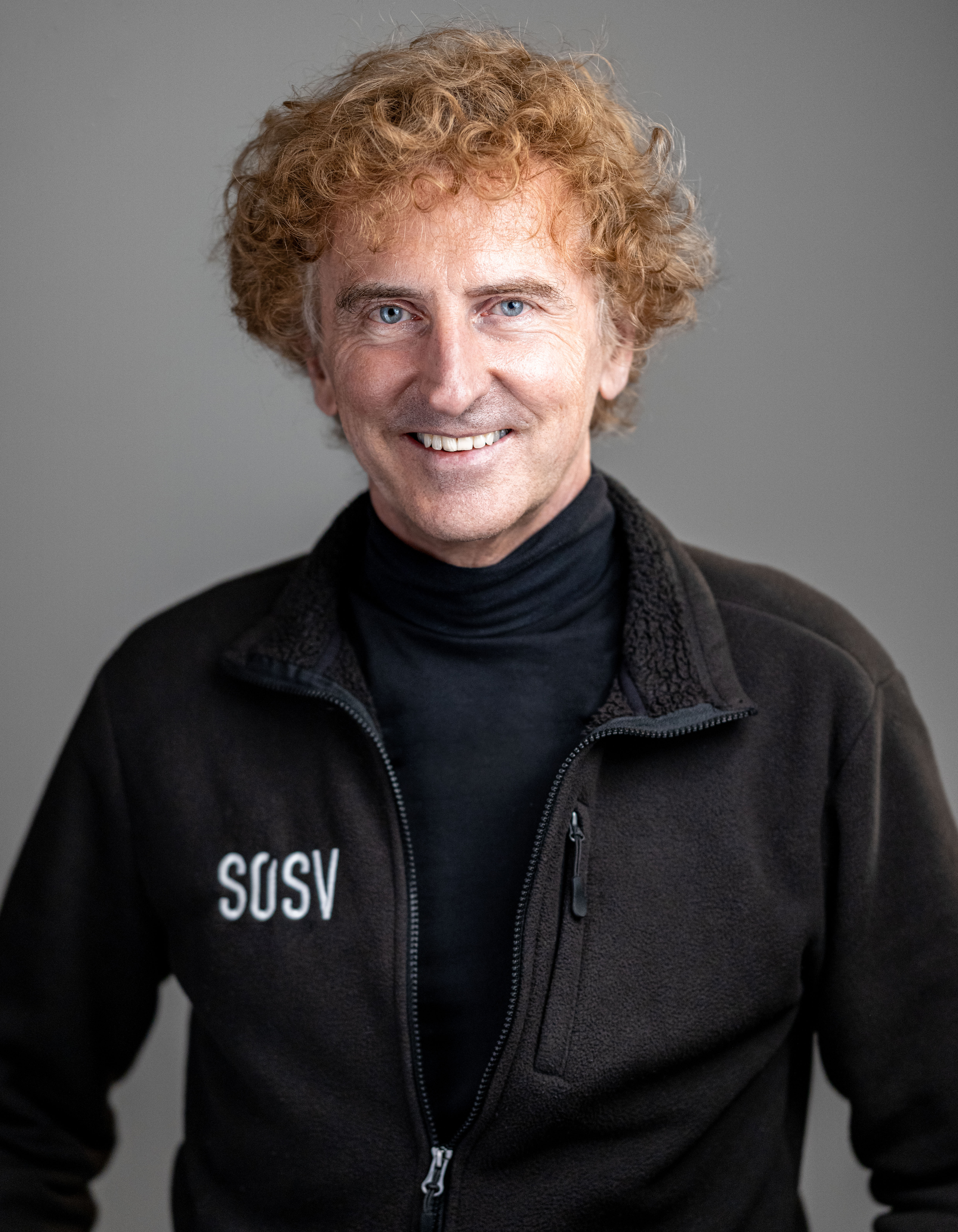
Founder and Managing General Partner
SOSV Princeton, NJ
Tuesday, April 16, 10:30 a.m.-noon. The event will include an open discussion/panel featuring SOSV leaders with Ohio State student and faculty entrepreneurs.
E100 Scott Laboratory
201 W. 19th Ave. Columbus, Ohio
Abstract
SOSV, the world’s most active investor in climate tech, as well as in deep tech and life sciences, backs around 70 new deep-tech startups a year. Sean O’Sullivan, the Managing General Partner and founder of SOSV, will take us through his personal journey becoming a venture capitalist, the themes for SOSV investment, and how we all can rethink “the means of production” of everything from food, to manufacturing, to materials, in order to stop producing the greenhouse gases (GHGs) that are threatening our planetary health.
The methods and materials we use today to create and build the world we live in produce excessive amounts of carbon emissions that are producing great change in how our planet, especially our climate, behaves. The planet’s resources are not enough for our population to continue growing and consuming at the rate at which we grow and consume today (we should have stopped at 2.5 billion in population if we didn’t want to create global warming). The increase in the world’s middle-class and their consumption levels will exacerbate the GHG emission crisis.
There are no easy or fantastical solutions to this problem. Sucking the carbon out the air is irrationally expensive and ineffective. If we want to save our planet, we need to transform our means of production. At SOSV, we invest in companies that are doing the hard, physical work of manufacturing the materials we need while producing less or even offsetting carbon emissions.
SOSV runs the IndieBio (life sciences) and HAX (chemistry, mechanical, electronics, physics) programs in various locations around the world, awarding up to $500k to startups in the first check, and following on with up to $7m in additional capital as the companies hit later stages, while helping bring billions of capital into the startups they back every year.
Speaker Bio
Sean O’Sullivan is Managing General Partner of SOSV, a venture capital firm with over $1.6 Billion in assets under management. O’Sullivan began as an entrepreneur, and his first startup, MapInfo, grew to a $200 million revenue public company with over 1,000 employees, popularizing street mapping on computers. His first internet company, NetCentric, developed many concepts in internet computing, and he is credited as the co-creator of the term “cloud computing”. He received his BS in Electrical Engineering from Rensselaer Polytechnic Institute and a MFA in Film Production from the University of Southern California. As the founder of the O’Sullivan Foundation, he was the founding funder of Coderdojo (a global network of coding clubs that more than 50,000 kids attend every week) and is a principal donor to Khan Academy (used by more than 75 million students monthly). O’Sullivan is on the board of Khan Academy, the Tyndall Institute, the Autism Impact Alliance, the Brain Foundation, and private companies.
The Unprecedented Promise of Perovskite Photovoltaics
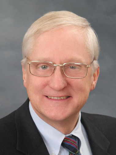
Nitin P. Padture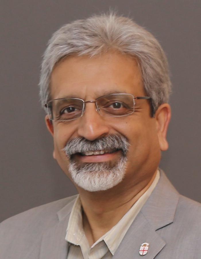
Otis E. Randall University Professor, School of Engineering
Director, Initiative for Sustainable Energy
Brown University
Thursday, Oct. 5, 2023 at 10:30 a.m. Reception to follow.
E100 Scott Laboratory
201 W. 19th Ave. Columbus, Ohio
Abstract
Perovskite solar cells (PSCs), a burgeoning thin-film photovoltaic (PV) technology, offers unprecedented promise of low-cost, high-efficiency renewable electricity generation. Metal-halide perovskite (MHP) light-absorbers at the heart of PSCs have unique crystal structures, which entail rotating organic cations inside inorganic cages, imparting them with highly desirable optical and optoelectronic properties. However, stability and mechanical reliability are becoming ‘bottleneck’ challenges in PSCs. This is because the low formation-energies of MHPs that make them easy to solution-process into thin films at near room-temperature also make them unstable and mechanically fragile. To address some of these technical hurdles in the path towards PSCs commercialization, several rationally-designed microstructural and interfacial tailoring approaches are used. These include grain-coarsening, grain-boundary functionalization, and interfacial engineering using self-assembled monolayers (SAMs). Most importantly, these approaches are designed to not only enhance the PSCs’ mechanical reliability but also increase efficiency and improve stability simultaneously. The scientific rationales for these approaches are discussed, together with the presentation of current results, in the context of the unprecedented promise offered by perovskite PVs.
Speaker Bio
Nitin P. Padture is the Otis E. Randall University Professor in the School of Engineering, and founding Director of the Initiative for Sustainable Energy (ISE), at Brown University. Previously he served as Director of Brown’s Institute for Molecular and Nanoscale Innovation (IMNI) for eight years. Prior to January 2012, he was College of Engineering Distinguished Professor at OSU, and also founding Director of OSU’s Center for Emergent Materials (CEM). Padture’s research and teaching interests are in the broad areas of advanced ceramics, semiconductors, and nanomaterials used in applications ranging from jet engines to solar cells. He has 280 publications to his credit, which have been widely cited (Google Scholar h-index 92), and he has presented 270 invited/keynote/plenary talks in the US and abroad. Padture is Fellow of the American Ceramic Society, the American Association for the Advancement of Science, and the Materials Research Society. His recent awards include Indian Institute of Technology – Bombay Distinguished Alumnus Award and Brown’s Presidential Faculty Award. Padture is Editor of two top journals in the field of materials science and engineering: Acta Materialia and Scripta Materialia.
Designer Nucleic Acid Architectures for Programmable Self-assembly
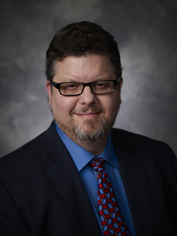
Hao Yan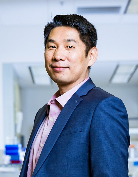
Milton D. Glick Distinguished Professor in Chemistry and Biochemistry and
Director of the Center for Molecular Design and Biomimetics in the Biodesign Institute
Arizona State University
Thursday, March 2, 2023 at 9:30 a.m. Reception to follow.
E100 Scott Laboratory
201 W. 19th Ave. Columbus, Ohio
Abstract
DNA and RNA has emerged as an exceptional molecular building block for nano-construction due to its predictable conformation and programmable intra- and inter-molecular base pairing interactions. A variety of convenient design rules and reliable assembly methods have been developed to engineer DNA nanostructures of increasing complexity. The ability to create designer DNA architectures with accurate spatial control has allowed researchers to explore novel applications in many directions, such as directed material assembly, structural biology, biocatalysis, DNA computing, nano-robotics, disease diagnosis, and drug delivery. In this talk I will discuss some of our work in the field of structural nucleic acid nanotechnology, and presents some of the challenges and opportunities that exist in DNA and RNA based molecular design and programming.
Speaker Bio
Hao Yan studied chemistry and earned his Bachelor’s degree at Shandong University, China. He obtained his PhD in Chemistry under Professor N. C. Seeman, New York University in 2001, working on design and construction of sequence dependent DNA nanomechanical devices. He then moved to the Computer Science Department at Duke University, where he continued to explore his interests in DNA based molecular computing and programming. Following a three year period as an Assistant Research Professor at Duke University, he joined Arizona State University as Assistant Professor in Department of Chemistry and Biochemistry in 2004. In 2008, he was promoted with early tenure directly to Full Professor and he is currently the Milton D. Glick Distinguished Professor in Chemistry and Biochemistry and Director of the Center for Molecular Design and Biomimetics in the Biodesign Institute at Arizona State University. The theme of his research is to use nature’s design rules as inspiration to advance biomedical, energy-related, and other technological innovations through the use of self-assembling molecules and materials. He aims to create intelligent materials with better component controls at the molecular level. He is leading an interdisciplinary team to design bio-inspired molecular building blocks and program their higher order assembly into systems that will perform complex functions. Dr. Yan has published more than 200 papers, including more than 40 papers published in journals such as Nature, Science, Cell and their sister Journals. He has received honors including the Foresight Institute Feynman Prize in Nanotechnology, the Rozenberg Tulip Award in DNA Computing, Alfred P. Sloan Research Fellowship, NSF Career Award, AFOSR Young Investigator Award. He has served as president of the International Society for Nanoscale Science, Computation and Engineering. He is an Elected Fellow of the National Academy of Inventors (NAI), the American Institute for Medical and Biological Engineering (AIMBE) and the American Association for Advancement of Science (AAAS). He currently serves as Associate Editor for Science Advances and ACS Applied Bio Materials.
Semiconductor Manufacturing and Design – How do we excite today’s students?
Mark E. Law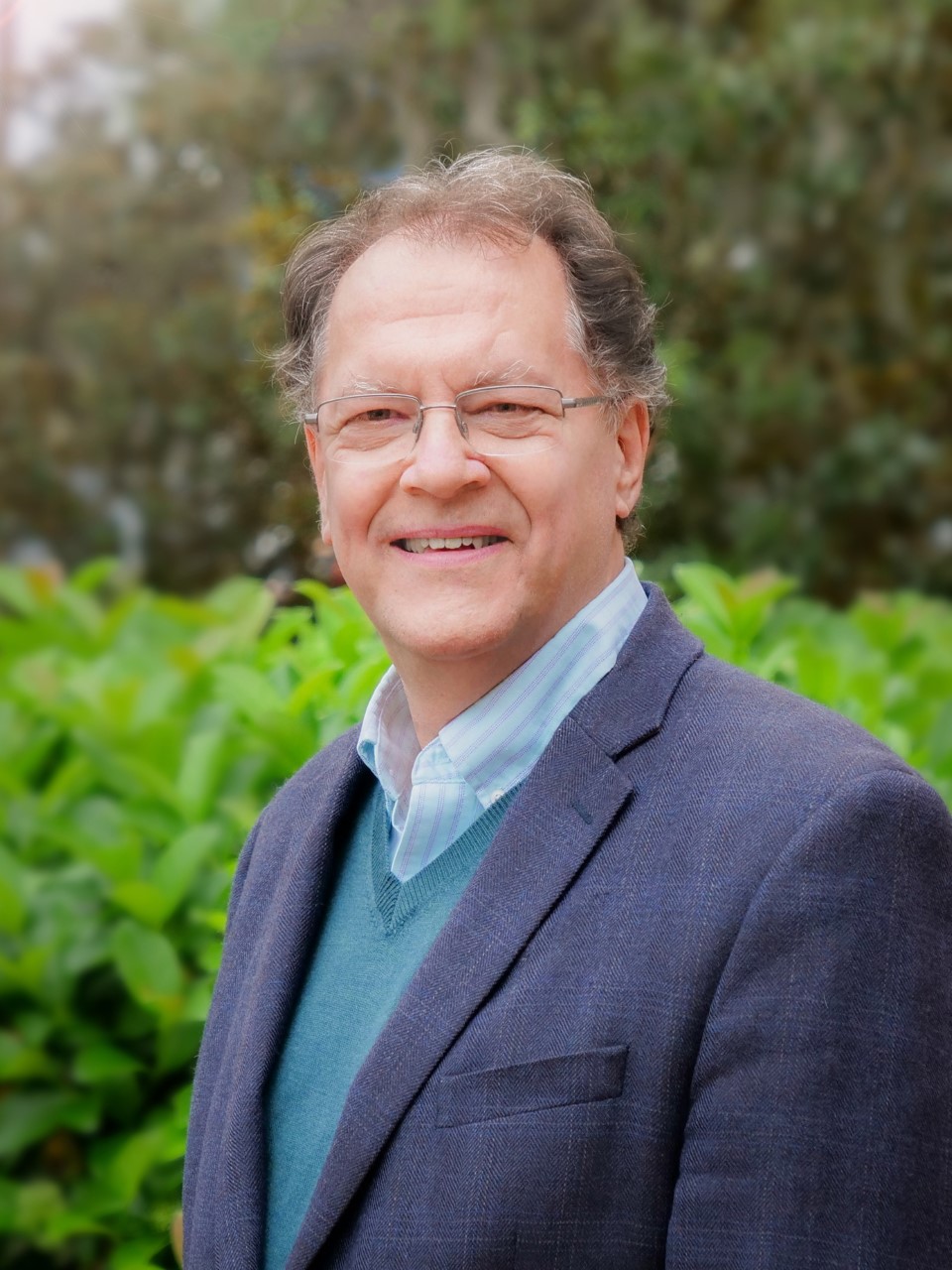
Distinguished Professor, University of Florida
Thursday, November 17, 2022 at 10:30 a.m. Reception to follow.
E100 Scott Laboratory
201 W. 19th Ave. Columbus, Ohio
Abstract
Today’s students have access to tools students 40 years ago could only dream of. They approach learning in different ways as well, but as a profession we largely teach in much the same way we did 40 or even 100 years ago. How can we engage students to want a career in semiconductor technology beyond a stable, well-paying job? How do we attract top students that seem to all want to be in health care? I’d like to highlight some approaches and ideas to help make semiconductors exciting and relevant again.
Speaker Bio
Dr. Mark Law is a distinguished and award-winning professor of electrical and computer engineering with a research emphasis in semiconductor devices and materials. For the last eight years, he has headed UF’s Honors Program which has provided him access and knowledge of students across disciplines.
New Materials and Devices for Quantum Coherent Technologies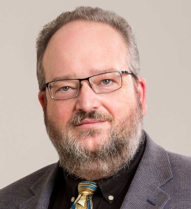
Michael E. Flatté
Professor in the Department of Physics and Astronomy
University of Iowa
Tuesday, October 15, 2019 at 3 p.m.
E100 Scott Laboratory
201 W. 19th Ave. Columbus, Ohio
Attendees are invited to join us for a brief reception and coffee following the talk in E100 Scott Laboratory.
Abstract
Over two decades ago concrete protocols were proposed to perform remarkable tasks, including breaking widely-used encryption, generating unbreakable codes, and rapidly searching huge databases. However, to achieve these goals new types of devices are required, relying on physical components with coherent quantum-mechanical properties that would persist for nearly unimaginably long times. The quest for materials and devices to achieve robust and versatile quantum coherent technologies has been filled with surprises, despite the reliance on so-called “mature materials” such as wide-gap semiconductors and low-temperature superconductors. A key research emphasis now is to meld the favorable properties of multiple materials or structures into hybrid coherent quantum systems that will outperform each of the constituents. I will describe some examples of the strengths and limitations of materials and devices technologies, and identify some of the features they share.
Speaker Bio
Michael E. Flatté is a professor at The University of Iowa (UI). His research interests include optical and electrical control of spin dynamics in materials, novel spintronic devices, quantum sensors, and solid-state realizations of quantum computation. He received an AB degree in physics from Harvard University in 1988 and a PhD degree in physics from the University of California, Santa Barbara (UCSB) in 1992. After postdoctoral work at the Institute for Theoretical Physics at UCSB and in the Division of Applied Sciences at Harvard University, he joined the faculty at UI in 1995. He was director of UI’s Optical Science and Technology Center from 2010 to 2017. Flatté has more than 200 publications and 10 patents. He is a Fellow of the American Association for the Advancement of Science and of the American Physical Society (APS), and was chair of the Division of Materials Physics of APS from 2016 to 2017. In 2019 he developed the first course on Quantum Engineering for the Pritzker School of Molecular Engineering at the University of Chicago. Flatté also has an adjunct appointment as professor in the Department of Applied Physics at Eindhoven University of Technology in the Netherlands.
Genomic Materials Design: From CALPHAD to Flight
GREGORY B. OLSON
Walter P. Murphy Professor of Materials Science and Engineering
Northwestern University
Co-founder and Chief Scientific Officer, QuesTek Innovations, LLC
Thursday, April 18, 2019 at 9:30 a.m.
E100 Scott Laboratory
201 W. 19th Ave. Columbus, Ohio
Abstract
Sixty years of academic collaboration and thirty years of commercialization by an international network of small businesses have delivered a mature technology of computational materials design and accelerated qualification grounded in a system of fundamental databases now known as the Materials Genome. Two computationally designed aircraft landing gear steels have already been taken to full flight qualification employing this technology. The announcement in 2011 by the US President of a national Materials Genome Initiative acknowledging the reality of this technology has spurred global interest and rapid adoption by US apex corporations. Designed materials with broad market impact now span a range from consumer electronics to space exploration. The US CHiMaD Center for Hierarchical Materials Design is expanding the capabilities of proven CALPHAD-based design with applications spanning inorganic and organic systems, while exploring new opportunities in high-throughput experiment and theory aided by novel data analytics. A major focus of current application is the rapid development of the new alloys enabling the much-desired technology of additive manufacturing, with adaptation of the AIM methodology to accelerate qualification of printed components. A research-supported hierarchical project coaching system has enabled multiyear interdisciplinary materials design education activities from freshman to doctoral levels.
Speaker Bio
Greg Olson is Co-director of the NIST-supported CHiMaD Center for Hierarchical Materials Design, Director of its SRG Design Consortium, and is a founder of QuesTek Innovations LLC, an internationally recognized leading materials design company. A member of the National Academy of Engineering, the American Academy of Arts and Sciences, the Royal Swedish Academy of Engineering Sciences, and a fellow of ASM and TMS, he has authored more than 300 publications. He received a BS and MS in 1970 and ScD in 1974 in materials science from MIT and remained there in a series of senior research positions before joining the faculty of Northwestern in 1988. Beyond materials design, his research interests include phase transformations, structure/property relations, and applications of high resolution microanalysis. Recent awards include the ASM Campbell Memorial Lectureship, the TMS-SMD Distinguished Scientist/Engineer Award, the Cambridge University Kelly Lectureship, the ASM Gold Medal, the TMS Morris Cohen Award, and an honorary doctorate from KTH-Stockholm.

Superconductivity: Where we are and where we are going
Robert J. Cava
Russell Wellman Moore Professor of Chemistry
Princeton University
Tuesday, Oct. 30, 2018, 1 p.m.
1080 Physics Research Building
(Smith Seminar Room)
191 W. Woodruff Ave., Columbus, Ohio
Abstract
The discovery of superconductivity, the transmission of electrical current with zero energy loss, recently passed its 100th anniversary. This truly remarkable property of matter, found at cryogenic temperatures, has made its way into a variety of important uses in modern society, but nature has not yet given us the ultimate practical material that will change the world through its lossless transmission of electrical energy over long distances. Research on this complex problem in materials science persists in the world at many levels, and progress is continuously made on both scientific and practical fronts, in spite of the impatience that is often displayed by both the scientific and lay public, who typically prefer immediate rather than delayed gratification. In this talk I will briefly describe where we are in this field, and how we got here, and describe the vision that some have had for where we should be going. Because my personal research is in the discovery of new superconducting materials, only one facet among the larger set of fundamental and practical issues currently under study, the talk will be given from that perspective.
Speaker Bio
Robert Cava is the Russell Wellman Moore Professor of Chemistry at Princeton University, where he is the former Chair of the Chemistry Department and former Director of the Materials Institute. His research in new materials emphasizes the relationships between chemistry, crystal structure, and electronic and magnetic properties. He received his Ph.D. in Ceramics from MIT in 1978, after which he was an NRC Postdoctoral Fellow in Solid State Chemistry at NIST. He began at Princeton in 1997 after working at Bell Labs for 17 years, where he was a Distinguished Member of Technical Staff. He is a Fellow of the American Physical Society, the American Ceramic Society, and the Neutron Scattering Society of America, and is a member of the U.S. National Academy of Sciences and a Foreign Member of The Royal Society of London. He has been the recipient of awards from the APS, the ACS, and the MRS, and has more than 60,000 citations.
High-K Dielectrics: A Perspective on Applications from Silicon to 2-D Materials
Robert M. Wallace
Professor of Materials Science and Engineering and Erik Jonsson Distinguished Chair in the Erik Jonson School of Engineering and Computer Science
University of Texas at Dallas
Tuesday, March 27, 2018, 2 p.m.
E100 Scott Laboratory
201 W. 19th Ave., Columbus, Ohio
Attendees are invited to join us for refreshments and appetizers following the talk at E100 Scott Lab.
Abstract
In the 1990s, research accelerated on addressing the limits of the industry standard gate dielectric: SiO2. With the most aggressive integrated circuit scaling, it became clear that standby power for MOSFETs required the insertion of a gate dielectric material that reduced tunneling leakage while enabling performance expectations. Leveraging prior dielectric research and after exploring several dielectric material candidates, [1,2] Hf-based dielectrics became the dominant choice and were established in commercial Si technology fabrication processes in 2007 after at least a decade of research. [3] Although perhaps forgotten among today’s 3-D FET technologies, the introduction of a new gate dielectric, simultaneously with metal gate materials, was considered quite revolutionary in its day, and this development, in conjunction with other device engineering aspects like strain, enabled the continued march of the industry along Moore’s original predictions. Since that time, the research on incorporating high-k dielectrics has expanded to address alternative channel materials including Ge, III-V, wide band gap semiconductors, and, most recently, perhaps the ultimate limit in channel scaling – atomically thin 2-D materials. [4] This talk, from the author’s perspective, will review some of these developments and provide some context on the resilience of the materials research as well as the challenges and opportunities that lie ahead. [5]
This work is supported in part by the US-Ireland R&D Partnership (UNITE) under the NSF award ECCS-1407765, and (iv) the Erik Jonsson Distinguished Chair in the Erik Jonson School of Engineering and Computer Science at the University of Texas at Dallas.
[1] J. Robertson and R.M.Wallace, Materials Science and Engineering R, 88, 1-41 (2015).
[2] G.D.Wilk, R.M.Wallace, and J.M.Anthony, Journal of Applied Physics 89 5243 (2001).
[3] M.T. Bohr, R.S. Chau, T. Ghani, K. Mistry, IEEE Spectrum. 44 (29) (2007).
[4] S.J. McDonnell and R.M.Wallace, Thin Solid Films, 616, 482 (2016).
[5] R.M.Wallace, ECS Transactions 80(1), 17 (2017).
Speaker Bio
Robert M. Wallace received his B.S. in Physics and Applied Mathematics in 1982 at the University of Pittsburgh where he also earned his M.S. (1984) and Ph.D. (1988) in Physics, under Prof. W. J. Choyke. From 1988 to 1990, he was a postdoctoral research associate in the Department of Chemistry at the Pittsburgh Surface Science Center under the late Prof. John T. Yates, Jr.
In 1990, he joined Texas Instruments Central Research Laboratories as a Member of Technical Staff (MTS) in the Materials Characterization Branch of the Materials Science Laboratory, and was elected as a Senior MTS in 1996. Dr. Wallace was then appointed in 1997 to manage the Advanced Technology branch in TI’s R&D, which focused on advanced device concepts and the associated material integration issues. In 2003, he joined the faculty in the Erik Jonsson School of Engineering and Computer Science at the University of Texas at Dallas (UTD) as a professor of Electrical Engineering and Physics. He is a founding member of the Materials Science and Engineering program at UTD and served as an interim head for the program. Dr. Wallace also has appointments in the Departments of Electrical Engineering, Mechanical Engineering, and Physics.
Research in the Wallace group focuses on the study of surfaces and interfaces, particularly with applications to electronic materials and the resultant devices fabricated from them. Current interests include materials systems leading to concepts that may enable further scaling of integrated circuit technology and beyond CMOS-based logic. These include the study of the surfaces and interfaces of compound semiconductor systems, including arsenides (e.g. InGaAs), nitrides (e.g. GaN), phosphides (e.g. InP), as well as antimondies (e.g. GaSb), and most recently 2-D materials, such as graphene and transition metal dichalcogenides. He has authored or co-authored over 375 publications in peer-reviewed journals and proceedings with over 20000 (29000) citations according to Scopus (Google Scholar).
Dr. Wallace is also an inventor on 45 U.S. and 27 international patents/applications, and a co-inventor of the Hf-based, high-k gate dielectric materials now used by the semiconductor industry for advanced high performance logic in microprocessors. He was named Fellow of the AVS in 2007 and an IEEE Fellow in 2009 for his contributions to the field of high-k dielectrics in integrated circuits.
The Influence of Fields and Dopants on Grain Boundary Mobility
Wayne D. Kaplan
Professor in the Department of Materials Science and Engineering
Technion – Israel Institute of Technology
Thursday, October 12, 2017
2 p.m.
E100 Scott Laboratory
Abstract
Controlling grain size is a fundamental part of Materials Science and Engineering. While the driving force for grain growth is thought to be understood, the mechanism by which grain boundaries migrate, and how microscopic parameters affect grain boundary mobility, are less understood. This presentation focuses on the mobility of grain boundaries and how dopants and external fields influence the kinetics of grain growth.
The first part of the talk will address the concept of solute-drag, where conventional wisdom indicates that moving a solute cloud with a grain boundary should either slow down grain boundary motion (e.g. Mg in Al2O3), or not affect it. Model experiments at dopant levels below the experimentally determined solubility limit clearly show that some adsorbates reduce grain boundary mobility (the accepted solute-drag effect) whereas other increase grain boundary mobility (solute-acceleration). Reasons for the varying behavior are discussed within the framework of grain boundary disconnections as the mechanism by which grain boundaries move, and current approaches to understanding Gibbsian adsorption.
The second part of the talk reviews model experiments designed to probe the influence of external fields on grain boundary mobility. As a model system, polycrystalline SiC underwent conventional annealing, and annealing using spark plasma sintering (SPS) without pressure, and the grain size as a function of annealing time was characterized. From these experiments, the grain boundary mobility of SiC at 2100°C under conventional versus SPS annealing was determined. SPS annealing resulted in a grain boundary mobility which is three orders of magnitude larger than that resulting from conventional annealing. This indicates that the same (or similar) mechanism which promotes rapid sintering during SPS also significantly increases the rate of grain growth. This mechanism will be discussed in light of the “solute-acceleration” effect presented in the first part of the talk.
Speaker Bio
Wayne D. Kaplan is a full professor in the Department of Materials Science and Engineering at the Technion – Israel Institute of Technology, where he holds the Karl Stoll Chair in Advanced Materials. Kaplan currently serves as the Executive Vice President for Research at the Technion. He completed his BSc in Mechanical Engineering, and his MSc and DSc in Materials at the Technion after immigrating to Israel from the U.S. He then spent a year as a Humboldt Fellow at the Max-Planck Institute in Stuttgart Germany before joining the Technion faculty in 1995.
During the past 20 years Kaplan’s research activities at the Technion have focused on the structure, chemistry and energy of interfaces between metals and ceramics, with a focus on the correlation between thermodynamics (continuum) approaches and the atomistic structure and chemistry of interfaces. In addition to his fundamental research in materials science, Kaplan works on the development of electron microscopy techniques for characterization at the sub-nanometer length-scale.
Kaplan is the author of more than 130 reviewed and archived scientific articles, as well as two textbooks: Joining Processes and Microstructural Characterization of Materials. In 2006 he received the Henry Taub Prize for Academic Excellence. He is a fellow of the American Ceramic Society, a member of the Israel Microscopy Society, and was an editor of the Journal of Materials Science (Springer).
From Mobile Phones to Russian Dolls to MASERs
Neil Alford
Head of Department of Materials
Imperial College London
Friday, January 20, 2017
9:30 AM
Smith Seminar Room, 1080 Physics Research Building
Abstract
In this talk we will look at the problem of dielectric loss (the tan δ) in oxides and how this led us to the world’s first room temperature MASER. Why are we interested in dielectric loss? Almost all of us have a mobile phone and dielectric resonators form essential parts of communications systems. The term “Dielectric Resonator” was first used by Richtmeyer(1) in 1939 who showed that a dielectric ring could confine high frequency electromagnetic waves and thus form a resonator. The idea of a dielectric material confining EM radiation dates back to 1897 when Lord Rayleigh described a dielectric waveguide(2) and in 1909 when Debye described dielectric spheres(3). With the astonishing growth in the cellular communications industry the market is now very approximately 2BN sales of mobile phones each year (that’s about 60 each second) the market for microwave ceramics is huge.
World’s first room temperature, Earth’s field MASER
One of the key properties is the dielectric loss or tan delta. The inverse of this is called the Quality factor or Q. Imagine a tuning fork. When you strike it, it resonates for a long time – it has a high Q and if it were made from e.g. wood it would be damped severely, would not resonate and have a very low Q. Now imagine hitting a dielectric (like alumina or sapphire) with an electromagnetic wave – a microwave – it resonates and what we need is a very high Q so that we can build good filters. The dielectric loss is limited by the dielectric loss of the material – the dielectric limit – but suppose you could exceed this. This is what we did by some cunning engineering using a Bragg reflector (a bit like a Russian doll) in which the sapphire layers of the Russian doll (called Bragg layers) are not the usual equal thickness but are aperiodic. Remarkably, if the layers are aperiodic in thickness the Q factor rises quadratically to reach extraordinarily high values of Q=0.6×10⁶ at 30GHz (world record)(4).
This result suggested that it might be possible to reach the threshold for masing and indeed we demonstrated that in P-terphenyl doped with pentacene when located inside a very high Q sapphire resonator maser action can be observed. This is the first time a solid state maser has been demonstrated at room temperature and in the earth’s magnetic field(5). Recent work(6) has shown that miniaturisation is feasible and considerable reduction in pumping power is possible by using a strontium titanate resonator which by virtue of a higher relative permittivity leads to a factor of over 5 in size reduction. Importantly, the Purcell factor which is the ratio of the Q factor to the mode volume, remains high and this is a key factor in the ability to exceed the threshold for masing.
Speaker Bio
Professor Neil Alford MBE FREng is a materials scientist and Associate Provost for Academic Planning at Imperial College London. He worked in industry for 15 years and then in University research at Queen Mary College, Oxford and South Bank University. His work has focused on materials from high-strength cement to High Temperature Superconductors, nanotechnology and room temperature MASERs. Technology transfer is a key focus and Neil’s discoveries been applied widely in industry, including cellular communications. Having held various academic posts at Imperial (including HoD of Materials), Neil is closely involved in the College’s new White City Campus. Spanning 23 acres, the campus will provide a new research and innovation district, where Imperial and its partners work to tackle the world’s greatest challenges. It will provide space for new types of multidisciplinary research, collaboration with corporations, institutions and start-ups, as well as activities to engage and inspire the community in White City.
1. R. D. Richtmeyer, J Appl. Phys. 10, 391-398 (1939)
2. Lord Rayleigh, Phil. Mag. S.5 43, 125-132 (1897)
3. P. Debye, Ann. D. Physik, 30, 57-136 (1909)
4. Better than Bragg: Optimizing the quality factor of resonators with aperiodic dielectric reflectors Breeze Jonathan; Oxborrow Mark; Alford Neil McN APPLIED PHYSICS LETTERS Volume: 99 Issue: 11 Number: 113515 2011
5. Room Temperature Maser NATURE, 16 August 2012 Mark Oxborrow, Jonathan Breeze and Neil Alford
6. Enhanced magnetic Purcell effect in room-temperature masers Jonathan Breeze, Ke-Jie Tan, Benjamin Richards, Juna Sathian, Mark Oxborrow and Neil Alford Nature Comms DOI 10.1038/ncomms7215 (2015)
21.25% World Efficiency Record with Multi-Crystalline p-type Silicon Solar Cells: Closing the Gap with n-type Mono
 Pierre Verlinden, Vice President, Chief Scientist and Vice-Chair of State Key Laboratory, Trina Solar
Friday, June 17, 2016
10:00 AM (Reception to follow)
E525 Scott Laboratory, 201 West 19th Avenue
Abstract
Multicrystalline Silicon technologies represents more than 65% of 2015 global shipments. Over the last two years, the best p-type multicrystalline silicon solar cells developed by Trina Solar have reached new efficiency records, up to 20.86% in 2014 and 21.25% in 2015. These achievements result from improvements of all aspects of the solar cell fabrication: contamination control, development of high-performance multi-crystalline silicon wafers, cell design and process optimization. Analysis show that efficiencies above 22% are possible with p-type multicrystalline and could be reached in the next few years.
Speaker Bio
Pierre J. Verlinden is Vice-President and Chief Scientist at Trina Solar, the world’s largest PV manufacturer. He is also Vice-Chair of the State Key Laboratory of PV Science and Technology. Dr. Verlinden has been working in the field of photovoltaics for more than 35 years and has published over 170 technical papers and contributed to a number of books. Before joining Trina Solar, Dr. Verlinden served as Chief Scientist or head of R&D department in several other PV companies in USA and Australia, including SunPower, Origin Energy, Amrock and Solar Systems.
Antimonide Materials for Mid-Infrared Photonic Detectors and Focal Plane Arrays
 Sanjay Krishna, Director, Center for High Technology Materials, Professor and Regents’ Lecturer, Department of Electrical and Computer Engineering, University of New Mexico
Tuesday, April 12, 2016
9:45 AM (reception to follow)
E100 Scott Laboratory, 201 West 19th Avenue
Abstract
Infrared imaging (3-25mm) has been an important technological tool for the past sixty years since the first report of infrared detectors in 1950s. There has been a dramatic progress in the development of infrared antimonide based detectors and low power electronic devices in the past decade with new materials like InAsSb, InAs/GaSb superlattices and InAs/InAsSb superlattices demonstrating very good performance. One of the unique aspects of the 6.1A family of semiconductors (InAs, GaSb and AlSb) is the ability to engineer the bandstructure to obtain designer band-offsets. Our group (www.krishnairlab.com) has been involved with the vision of the 4th generation of infrared detectors and is one of two university laboratories in the country that can undertake “Design to Camera” research and realize focal plane arrays.
This talk will revolve around three research themes:
The first theme involves the fundamental investigation into the material science and device physics of the antimonide systems. I will describe some of the challenges in these systems including the identification of defects that limit the performance of the detector. The use of “unipolar barrier engineering” to realize high performance infrared detectors and focal plane arrays will be discussed.
The second theme will involve the vision of the 4th Gen infrared imaging systems. Using the concept of a bio-inspired infrared retina, I will make a case for an enhanced functionality in the pixel. The key idea is to engineer the pixel such that it not only has the ability to sense multimodal data such as color, polarization, dynamic range and phase but also the intelligence to transmit a reduced data set to the central processing unit. The design and demonstration of meta-infrared detectors will be discussed.
In the final theme, I will describe the role of infrared imaging in bio-medical diagnostics. In particular, I will highlight some work on using infrared imaging in the early detection of skin cancer and for detection of flow in cerebral shunts. Using dynamic thermal imaging on over 100 human subjects, a sensitivity >95% and specificity >83% has been demonstrated. Commercialization of this technology will also be discussed.
Speaker Bio
Sanjay Krishna is the Director of the Center for High Technology Materials and Professor and Regents Lecturer in the Department of Electrical and Computer Engineering at the University of New Mexico. Sanjay received his M.S. from IIT, Madras, MS in Electrical Engineering in 1999 and PhD in Applied Physics in 2001 from the University of Michigan. He joined UNM as a tenure track faculty member in 2001. He currently heads a group of 15 researchers involved with the development of next generation infrared imagers. Sanjay received the Gold Medal from IIT, Madras, Ralph Powe Junior Faculty Award, IEEE Outstanding Engineering Award, ECE Department Outstanding Researcher Award, School of Engineering Jr Faculty Teaching Excellence Award, NCMR-DIA Chief Scientist Award for Excellence, the NAMBE Young Investigator Award, IEEE-NTC, SPIE Early Career Achievement Award and the ISCS Young Scientist Award. He was also awarded the UNM Teacher of the Year and the UNM Regents Lecturer award. Sanjay has more than 200 peer-reviewed journal articles (h-index=42), two book chapters and seven issued patents. He is the co-founder and CTO of Skinfrared, a UNM start-up involved with the use of IR imaging for dual use applications including early detection of skin cancer. He is a Fellow of IEEE, OSA and SPIE.
 Ionic Liquids for Post-Combustion CO2 Capture
Joan F. Brennecke
Keating-Crawford Professor of Chemical Engineering
Department of Chemical and Biomolecular Engineering
University of Notre Dame
Wednesday, February 18, 2015
Abstract
Ionic liquids (ILs) present intriguing possibilities for removal of carbon dioxide from a wide variety of different gas mixtures, including post-combustion flue gas, pre-combustion gases, air, and raw natural gas streams. Even by physical absorption, many ILs provide sufficient selectivity over N2, O2, CH4 and other gases. However, when CO2partial pressures are low, the incorporation of functional groups to chemically react with the CO2 can dramatically increase capacity, while maintaining or even enhancing selectivity. We will demonstrate several major advances in the development of ILs for CO2capture applications. First, we will show how the reaction stoichiometry can be doubled over conventional aqueous amine solutions to reach one mole of CO2 per mole of IL by incorporating the amine on the anion. Second, we will show how we have been able to virtually eliminate any viscosity increase upon complexation of the IL with CO2, by using aprotic heterocyclic anions (AHA ILs) that eliminate the pervasive hydrogen bonding and salt bridge formation that is the origin of the viscosity increase. Third, we will describe the discovery of AHA ILs whose melting points when reacted with CO2 are more than 100 °C below the melting point of the unreacted material. These materials allow one to dramatically reduce the energy required for CO2 release and regeneration of the absorption material because a significant amount of the energy needed for the regeneration comes from the heat of fusion as the material releases CO2 and turns from liquid to solid.
Speaker Bio
Joan F. Brennecke is the Keating-Crawford Professor of Chemical Engineering at the University of Notre Dame and was the founding Director of the Center for Sustainable Energy at Notre Dame. She joined Notre Dame after completing her Ph.D. and M.S. (1989 and 1987) degrees at the University of Illinois at Urbana-Champaign and her B. S. at the University of Texas at Austin (1984).
Her research interests are primarily in the development of less environmentally harmful solvents. These include supercritical fluids and ionic liquids. In developing these solvents, Dr. Brennecke’s primary interests are in the measurement and modeling of thermodynamics, thermophysical properties, phase behavior and separations. Major awards include the 2001 Ipatieff Prize from the American Chemical Society, the 2006 Professional Progress Award from the American Institute of Chemical Engineers, the J. M. Prausnitz Award at the Eleventh International Conference on Properties and Phase Equilibria in Greece in May, 2007, the 2008 Stieglitz Award from the American Chemical Society, the 2009 E. O. Lawrence Award from the U.S. Department of Energy, and the 2014 E. V. Murphree Award in Industrial and Engineering Chemistry from the American Chemical Society. She serves as Editor-in-Chief of the Journal of Chemical & Engineering Data. Her 130+ research publications have garnered over 12,000 citations. She was inducted into the National Academy of Engineering in 2012.
The Automotive Industry, Vehicle Electrification, and Industrial Research
Mark W. Verbrugge
Chemical and Materials Systems Laboratory
General Motors Research and Development
Tuesday, October 14, 2014
Abstract
This talk will begin with a review of automotive vehicle electrification: trends and drivers. The life of lithium-ion batteries is related to the mechanical expansion and contraction of the active materials along with solvent decomposition at the active material surfaces—lithium-ion batteries would not work if a protective shell did not cover the electroactive core of the positive and negative electrode materials. Exposure of the active core leads to cell degradation. These observations hold for current and next-generation lithium-ion batteries. Under what conditions are the protective (outer shell) materials compromised? In addition to reviewing literature that is relevant to answering this question, the speaker intends to overview research results to render a qualitative response to this question and identify open questions that limit the quantitative application of modeling results to these systems. Last, we will close with a brief perspective on “what is useful industrial research?”
Speaker Bio
Mark Verbrugge is the Director of GM’s Chemical and Materials Systems Laboratory, which maintains global research programs—enabled by the disciplines of chemistry, physics, and materials science—and targets the advanced development of structural subsystems, energy storage and conversion devices, and various technologies associated with fuels, lubricants, and emissions.
Mark is a Board Member of the United States Automotive Materials Partnership LLC and the United States Advanced Battery Consortium LLC. Mark has received a number of GM internal awards as well as external awards including the Norman Hackerman Young Author Award and the Energy Technology Award from the Electrochemical Society, and the Lifetime Achievement Award from the United States Council for Automotive Research. Mark is a Fellow of the Electrochemical Society and a member of the National Academy of Engineering.
Silicon Photovoltaics: Power Source for the Future?
Prof. Martin A. Green
Australian Centre for Advanced Photovoltaics, School of Photovoltaic and Renewable Energy Engineering
University of New South Wales, Australia
Monday, October 7, 2013
Abstract
The last few years has seen photovoltaics (PV) emerge from relative obscurity to becoming one of the top three sources of new electricity generation capacity internationally. The vast majority of photovoltaic solar cells produced to date have been based on silicon wafers, with this dominance likely to continue well into the future. The surge in manufacturing volume over the last decade has resulted in greatly decreased costs. Multiple companies are now producing at costs much lower than the US$1/Watt module manufacturing cost benchmark once regarded as the lowest possible with this technology. Despite these huge cost reductions, there is clear scope for much more, as the polysilicon source material becomes more competitively priced, new “high-performance” directional solidification processes for producing increasingly large and better-performing silicon ingots are brought on-line, wafer slicing switches to much quicker diamond impregnated approaches and cell conversion efficiencies increase towards 25% and increasing effort is placed on the development of even higher performance silicon-based tandem cell stacks. Photovoltaics are increasingly seen as a viable green energy source of the future, meeting growing energy demands on a large scale without adding to the carbon burden.
Speaker Bio
Dr. Martin Green is currently Scientia Professor at the University of New South Wales, Sydney and Director of the Australian Centre for Advanced Photovoltaics. His group’s contributions to photovoltaics include development of the world’s highest efficiency silicon cells and commercialization of several different cell technologies. He is the author of several books on solar cells and numerous papers. His work has been recognised by major international awards including the 2002 Right Livelihood Award, also known as the Alternative Nobel Prize, the 2007 SolarWorld Einstein Award and the 2010 Eureka Prize for Leadership. In 2012, he was appointed as a Member of the Order of Australia in recognition of his contributions to photovoltaics and photovoltaics education.
Past IMR Colloquia
From 2007 – 2013, the IMR hosted an IMR Colloquia Series that brought materials researchers from a broad range of fields to the OSU campus. This series has been replaced with the IMR Distinguished Lecture Series, and this information is provided for reference.
Two-Dimensional Electron Gases at Complex Oxide Interfaces
 Susanne Stemmer
Professor
Materials Department
University of California Santa Barbara
Thursday, April 11, 2013
Abstract: Two-dimensional electron gases at interfaces between two insulating oxides have attracted significant attention because they can exhibit unique properties, such as strong electron correlations, superconductivity and magnetism. In this presentation, we will discuss an example for such an interface, between the strongly correlated Mott insulator GdTiO3 and the band insulator SrTiO3. A fixed polar charge exists at these interfaces because of a polar discontinuity at the interface. The interfacial charge can be compensated by a high-density, two-dimensional electron gas (2DEG). At GdTiO3/SrTiO3interfaces grown by molecular beam epitaxy, this results in a high-density 2DEG, of approximately 1/2 electron per surface unit cell, or 3×1014 cm-2, for all GdTiO3/SrTiO3heterostructures, independent of the individual layer thicknesses and growth sequences. We will present measurements of quantum oscillations that provide insights into the nature of a 2DEG derived from the Ti d-states. We will report on electron correlation effects, such as magnetism and mass enhancement, in extremely high carrier density SrTiO3 quantum wells that can be obtained using these interfaces. Finally, we discuss the potential of oxide heterostructures for future electronic devices. The work was done in collaboration with Pouya Moetakef, Clayton Jackson, Tyler Cain, Leon Balents, Jim Allen, Jimmy Williams and David Goldhaber-Gordon.
Speaker Bio: Susanne Stemmer is Professor of Materials at the University of California, Santa Barbara. She received her Diploma in Materials Science from the Friedrich-Alexander University Erlangen-Nürnberg (Germany) and did her doctoral work at the Max-Planck Institute for Metals Research in Stuttgart (Germany). She received her doctoral degree from the University of Stuttgart in 1995. Following several postdoctoral positions she held an Assistant Professor position in Materials Science at Rice University from 1999 to 2002. In 2002, she joined the University of California, Santa Barbara, where she was promoted to Full Professor in 2008. Her research interests are in transmission electron microscopy techniques, in particular, the development of scanning transmission electron microscopy as a quantitative tool in materials science, novel dielectrics, oxide thin film growth and correlations between microstructure and electronic, dielectric and transport properties of oxide heterostructures. She has authored or co-authored more than 150 publications. Honors include an NSF Career Award, Fellow of the American Ceramic Society and Fellow of the American Physical Society.
Emerging Trends in AlInGaN Material and Devices Research 
Asif Khan
Director of Photonics and Microelectronics Laboratory, Distinguished Professor of Engineering, Carolina Distinguished Professor, University of South Carolina Department of Electrical Engineering
Thursday, October 4, 2012
Abstract: AlInGaN materials and devices research has come a long ways since its infancy days in the early 80′s. High power visible light emitting diodes and lasers have already become a multi-billion dollar business. For the power electronics market place, several large companies are now introducing components and modules based on AlInGaN HEMTs. There are all the indications that high-efficiency AlInGaN based electronic devices will also be a key player in these very large rf– and the low-frequency power electronics’ markets. In this presentation we will review the recent progress and discuss the emerging trends in the AlInGaN Optical and Electronic devices’ research. Our pioneering research at the University of South Carolina which led to the first demonstration and the improvement of power-lifetime performance in deep UV Light emitting diodes for air-water purification and bio-medical instrumentation will be discussed. Some of our recent work in insulating gate-enhancement mode AlIN-GaN HEMTs on silicon and other substrates will also be reviewed. In addition we will describe the innovative material growth strategies that led to low-defect epi-structures which are key to yielding the improved performance in AlInGaN Optical /Electronic devices.
Bio: Dr. Asif Khan is a Professor of Electrical Engineering and is the founding Director of the Photonics & Microelectronics Laboratory at the University of South Carolina. He has served as Professor (1997-present) and Department Chair (2001-2006) during his tenure. His research focus at USC is on the fabrication of GaN-AlGaN based high power microwave transistors and deep ultraviolet light emitters. A graduate of MIT, Dr. Khan has also worked for Honeywell, 3M, and a startup APA Optics. He has authored over 400 refereed papers, several book chapters, over 100 invited papers, and more than thirty patents. Among a long list of honors and awards, he has been selected as an IEEE Fellow, Plenary Speaker for numerous conferences and a DARPA Award for Outstanding Performance. He was also awarded Best Research Paper of the year in 2004 and 2006 by the Japanese Applied Physics Society, an honor given for pioneering research in AlInGaN LEDs. Dr. Khan’s resume has a long list of “Firsts” in research accomplishments as well as significant commercial products to his credit. His research groups pioneered GaN-Electronics and deep-ultraviolet LEDs. These products have blossomed into billion dollar industries. Dr. Khan was a founding member of two startups in Columbia SC namely SET Inc and Nitek Inc. These startups have led to more than 100 high-tech jobs in the state of South Carolina. They also provide excellent job opportunities for USC graduates thereby keeping their talents locally.
Materials Tomography and Femtosecond Lasers
Tresa M. Pollock
Alcoa Professor of Materials and Department Chair, Materials Department, University of California Santa Barbara
Thursday, May 10, 2012
Abstract: Optimization of the topological features of materials is often key to achieving exceptional material properties. Several examples of the use of 3-D structural information for materials optimization will be shown. A grand challenge, however, is efficient acquisition of 3-D materials information. A new tomography approach for nm-scale characteriztion of materials over mm3-scale volumes will be presented. The use of femtosecond lasers allows for in-situ layer-by-layer material ablation with high material removal rates. The high pulse frequency (1 kHz) of ultra-short (150 fs) laser pulses can induce material ablation with virtually no thermal damage to the surrounding area. This technique has been demonstrated ex-situ with optical imaging and more recently in-situ with a “TriBeam” approach that combines the femtosecond laser within a focused ion beam platform to permit high resolution imaging, as well as crystallographic and elemental analysis. Early 3D datasets from the TriBeam system demonstrate acquisition rates 4 to 6 orders of magnitude faster than focused ion beam systems.
Bio: Tresa Pollock is the Alcoa Professor of Materials and Department Chair at the University of California, Santa Barbara. She graduated with a B.S. from Purdue University in 1984, and a Ph.D. from MIT in 1989. Dr. Pollock was employed at General Electric Aircraft Engines from 1989 to 1991, where she conducted research and development on high temperature alloys for aircraft turbine engines. She was a professor in the Department of Materials Science and Engineering at Carnegie Mellon University from 1991 to 1999 and the University of Michigan from 2000 – 2010. Her current research focuses on the processing and properties of structural materials and coatings and on the use of ultrafast lasers for microfabrication and materials diagnostics. Professor Pollock was elected to the U.S. National Academy of Engineering in 2005, is a Fellow of TMS and ASM International, Associate Editor of Metallurgical and Materials Transactions and was the 2005-2006 President of The Minerals, Metals and Materials Society.
Made in the U.S.A. – Photovoltaic Energy Solutions
John P. Benner, Executive Director, Bay Area Photovoltaic Consortium and Stanford University
Tuesday, March 6, 2012
Download this presentation here
Abstract: News of excess production capacity, predatory pricing, and bankruptcies in the solar energy business have replaced the exhilaration over 65% compound annual growth rates, record stock valuations and announcements of large-scale photovoltaic applications. However, rumors of the death of this industry are greatly exaggerated. The photovoltaic business is healthy with enviable growth rates advancing technology on a trajectory to deliver electricity at prices on par with utility rates before 2020. Unfortunately, U.S. market share of photovoltaic module production continues to decline, clouding the vision of a nation moving toward energy self-sufficiency. To address this challenge, the Department of Energy launched the SunShot Initiative. Advanced Manufacturing Partnerships, the largest project in SunShot, include a University-Focused topic to support universities in industry-relevant R&D, guided by industry members. The challenge demands great innovation, as the dominant producer, China, provides manufacturers with substantial benefits from fewer restrictions, faster permitting processes, lower cost labor, a complete and local supply chain and substantial financial incentives. U.S. manufacturing leadership must be built upon superior, more innovative technologies delivered at all stages of the value chain. Great innovation is frequently traced to events bringing together individuals from diverse backgrounds. The Bay Area Photovoltaic Consortium (BAPVC) provides a vibrant forum for interaction among industry and academic experts to address critical challenges in PV manufacturing. BAPVC will find and fund the best university research teams to develop materials, device structures and processes for manufacturing by our industry members. This presentation will discuss the innovation, infrastructure and incentives needed to build a leading photovoltaic manufacturing base in the United States.
Bio: John Benner is the Executive Director of the Bay Area Photovoltaic Consortium (BAPVC), operated by Stanford University and the University of California Berkeley. BAPVC brings photovoltaic industry members together with leading university research teams to select and support research improving manufacture of photovoltaic modules. Benner began his work in photovoltaics during the formation of the Solar Energy Research Institute, now the National Renewable Energy Laboratory, where he served as project manager for high performance PV, Director of the Photovoltaic and Electronic Materials Center and Manager of PV Industry Partnerships.
Self-Assembly in Materials Chemistry
Samuel I. Stupp
Departments of Chemistry, Materials Science and Engineering, and Medicine, Northwestern University
Wednesday, November 9, 2011
Abstract: Self-assembly has emerged over the past two decades as a chemical strategy to create materials and devices. Based on lessons from biological systems, this strategy could be extraordinarily useful to craft highly functional materials from non-covalent assemblies of molecules and hybrid structures that imitate biomineralization. In order to harness the potential of the strategy in materials chemistry, the underlying science needed is a deep understanding of self-assembly codes based on both structure and external forces. So far self-assembly approaches have been developed mostly to organize molecules on surfaces, create supramolecular nanostructures with internal order, and to generate three dimensional patterns using phase separation of macromolecules. This lecture will illustrate self-assembly strategies to create more complex structures of interest in energy and medicine that have hierarchical order across scales. In these systems supramolecular self-assembly codes act synergistically with other forces to generate functional systems.
Bio: Professor Samuel Stupp is a native of Costa Rica and obtained his B.S. in chemistry at the University of California at Los Angeles, and his Ph.D. in materials science from Northwestern University. He spent 18 years at the University of Illinois at Urbana-Champaign where he was the Swanlund Professor of Materials Science, Chemistry, and Bioengineering. In 1999, he joined the faculty at Northwestern as Board of Trustees Professor of Materials Science, Chemistry, and Medicine, and later was appointed Director of Northwestern’s Institute for BioNanotechnology in Medicine. Professor Stupp is a member of the American Academy of Arts and Sciences and fellow of the American Physical Society, the Materials Research Society, the American Association for the Advancement of Science, the World Technology Network, and the World Biomaterials Congress. His awards include the Department of Energy Prize for Outstanding Achievement in Materials Chemistry, a Humboldt Senior Award, the Materials Research Society’s Medal Award, the American Chemical Society Award in Polymer Chemistry for his work on supramolecular self-assembly, and the Sir Edward Youde Memorial Award in Hong Kong. He has held the appointment of Joliot Curie Professor at Ecole Supérieure de Physique et de Chemie in Paris, Merck-Karl Pfister Visiting Professor in Organic Chemistry at MIT, Visiting Professor at the Institut de Science et d’Ingenierie Supramoléculaires in Strasbourg, and is currently Distinguished Professor of Eindhoven University of Technology in the Netherlands. In 2009, he received an honorary doctorate from Eindhoven University for revolutionary research in complex molecular systems and in 2011 an honorary doctorate from the National University of Costa Rica. His research is focused on self-assembly and supramolecular materials with special emphasis in regenerative medicine, cancer therapies, and solar energy.
Personalized Energy (for 1 x 6 Billion)
 Daniel G. Nocera, Henry Dreyfus Professor of Energy; Director, Solar Revolutions Project; Director, Eni Solar Frontiers Center, Massachusetts Institute of Technology
Tuesday, May 3, 2011
Abstract
The capture and storage of solar energy at the individual level – personalized solar energy – drives inextricably towards the heart of this energy challenge by addressing the triumvirate of secure, carbon neutral and plentiful energy. The doubling of global energy need by mid-century and tripling by 2100 is driven by 3 billion low-energy users in the non-legacy world and by 3 billion people yet to inhabit the planet over the next half century. The possibility of generating terawatts of carbon-free energy, and thus providing society with its most direct path to realizing a low GHG future, may be realized by making solar PE available to the 6 billion new energy users by high throughput manufacturing. This talk will present the creation of new catalysts for the oxygen evolving reaction (OER) and hydrogen evolving reaction (HER) that capture many of the functional elements of photosynthesis; these catalysts are then integrated to make the first artificial leaf. A movie will be shown of a OER/Si/HER wafer (no wires!) that sits in a glass of water and performs water splitting under one sun irradiation. It is indeed a leaf. The discovery sets a new paradigm for the direct production of solar fuels. In doing so, we provide a highly manufacturable and inexpensive method to effect a carbon-neutral and sustainable method for solar storage – solar fuels from water-splitting. By developing an inexpensive 24/7 solar energy system for the individual, a carbon-neutral energy supply for 1 × 6 billion becomes available.
Speaker Bio
Daniel G. Nocera is the Henry Dreyfus Professor of Energy at the Massachusetts Institute of Technology, Director of the Solar Revolutions Project and Director of the Eni Solar Frontiers Center at MIT. His group pioneered studies of the basic mechanisms of energy conversion in biology and chemistry. He has recently accomplished a solar fuels process that captures many of the elements of photosynthesis outside of the leaf and he has now translated this science to produce an artificial leaf. This discovery sets the stage for a storage mechanism for the large scale, distributed, deployment of solar energy. He has been awarded the Eni Prize, IAPS Award, Burghausen Prize, Harrison Howe Award, ACS Inorganic Chemistry Award and the United Nation’s Science and Technology Award for his contributions to the development of renewable energy. He is a member of the American Academy of Arts and Sciences and the U.S. National Academy of Sciences. He was named as one of Time Magazine’s 100 Most Influential People in the World and was 11th on the New Statesman’s list of the Most Influential People in the World. Nocera is a frequent guest on TV, he is regularly featured in print and he was in the feature length film Cool It, which premiered in the U.S. in November 2010. His 2006 PBS show was nominated for an Emmy Award, and it was used as a pilot to launch the PBS NOVA show, ScienceNow. In 2008, he founded Sun Catalytix, a company committed to bringing personalized energy to the non-legacy world.
The convergence of science and engineering: Energy conversion at nano scale
Fritz B. Prinz
Finmeccanica Professor of Engineering and Robert Bosch Chair, Department of Mechanical Engineering, Stanford University
Wednesday, November 10, 2010
Abstract: Selective mass and charge transfer drive energy conversion in any living system. Not unlike nature, man-made energy conversion systems such as fuel cells depend on membranes with selective ionic conduction.
Our experiments have shown that we can fabricate freestanding oxide membranes with a thickness of tens of nanometers. In particular, we used Yttria stabilized Zirconia and Gadolinia doped Ceria as electrolyte membranes for the creation of a new class Solid Oxide Fuel Cells (SOFCs) that are capable of operating at several hundred degrees centigrade below the temperature of traditional SOFCs. First principles calculations help in understanding oxide ion incorporation and ion conductivity as a function of dopant concentration.
Our ability to effectively draw power from ultra thin membrane structures inspired us to explore interrupting the natural electron transport chain in thylakoid membranes, the key ingredient of every chloroplast organelle in light sensitive plant cells. Exposing thylakoid membrane stacks to nano-scale electrodes and stimulating them with light pulses resulted in measurable polarization currents.
Speaker Bio: Fritz Prinz serves on the faculties of Mechanical Engineering and Materials Science and Engineering. He also holds the Finmeccanica Professorship in the School of Engineering. He obtained his Ph.D. in Physics at the University of Vienna, Austria. Prof. Prinz’s current work focuses on scaling effects and quantum confinement phenomena for energy conversion. His graduate students study mass transport phenomena across thin membranes such as oxide films and lipid bi-layers. In their research, the Prinz group employs Scanning Probe Microscopy, Impedance Spectroscopy, and Quantum Modeling. In his laboratory, prototype fuel cells, solar cells, and batteries serve to test new concepts and novel material structures.
Engineering the Future of Human Health
Dr. Subra Suresh, Massachusetts Institute of Technology
Dean of Engineering, Vannevar Bush Professor of Engineering
Wednesday, May 5th, 2010
This colloquium is co-sponsored by the Center for Emergent Materials, OSU’s NSF MRSEC Program.
Abstract: This lecture will describe recent research results and technological advances at the intersections of engineering, nanotechnology, genetics, life sciences, medicine and public health. Particular attention will be devoted to the role research at the intersections of these different fields plays in advancing the boundaries of human disease diagnostics, therapeutics and drug efficacy assays, through experiments, computations, and clinical studies. Specific examples will include research results for infectious diseases, human cancer, blood disorders and traumatic brain injury.
Biography: Subra Suresh is the Dean of Engineering and Vannevar Bush Professor of Engineering at the Massachusetts Institute of Technology, where he has held joint faculty appointments in Materials Science and Engineering, Mechanical Engineering, Biological Engineering, and Health Sciences and Technology. He is recognized internationally for his contributions to the areas of mechanical behavior of materials, fracture, fatigue, surface engineering, thin films, nanotechnology, and cell and molecular nanomechanics with particular connections to infectious diseases and cancer. His 225 journal articles, three authored books, and 16 patents have had a major impact on education, research and industrial practice in mechanical and aerospace applications, microelectronics, nanotechnology, materials science, and biomedical engineering.
Suresh has been elected to US National Academy of Engineering, American Academy of Arts and Sciences, Indian National Academy of Engineering, Indian Academy of Sciences, Royal Spanish Academy of Sciences, Academy of Sciences of the Developing World based in Trieste, Italy, and German National Academy of Sciences. He has been elected a Fellow or Honorary Member of all of the major materials professional societies in the USA and India. In 2006, MIT’s Technology Review magazine selected Suresh as one of the top 10 researchers whose work will have “significant impact on business, medicine or culture”. A recipient of the 2006 Acta Materialia Gold Medal, the 2007 European Materials Medal (the first non-European selected to receive this prize given jointly by co-operating materials professional societies from 27 European countries), the 2008 Eringen Medal of the Society of Engineering Science, and a Senior Humboldt Research Prize from Germany, Suresh has been awarded an honorary doctorate from Sweden’s Royal Institute of Technology. Spain’s Technical University of Madrid selected Suresh as the sole recipient for 2010 for its Doctor Honoris Causa degree “in recognition of his pioneering scientific contributions at the boundaries between materials engineering, mechanics, physics, biology and medicine”. From 2001-2006, Suresh served as the MIT Director and lead Principal Investigator of the Defense University Research Initiative in NanoTechnology, for a project funded by the Department of Defense through the National Nanotechnology Initiative.
Integrated Computational Materials Design
Gregory B. Olson
Wilson-Cook Chaired Professor in Engineering Design, Materials Science and Engineering, Northwestern University and Chief Science Officer, QuesTek Innovations LLC
Tuesday, February 9, 2010
Abstract: The numerical implementation of established materials science principles in the form of purposeful engineering tools has brought a new level of integration of the science and engineering of materials. Parametric materials design integrating materials science, applied mechanics and quantum physics within a systems engineering framework has brought a first generation of designer “cyberalloys” that have now entered successful commercial applications, and a new enterprise of commercial materials design services has steadily grown over the past decade. The success of materials design established a basis for the recent DARPA-AIM initiative which broadened computational materials engineering to address acceleration of the full materials development and qualification cycle. As the central engine of the AIM methodology, the PrecipiCalc microstructural simulator has demonstrated both accelerated thermal process optimization at the component level and the effective forecast of manufacturing variation with efficient fusion of minimal datasets. A new level of science-based modeling accuracy is being achieved under the ONR/DARPA “D3D” Digital Structure consortium using a suite of advanced 3D tomographic characterization tools to calibrate and validate a set of high fidelity explicit 3D microstructural simulation tools spanning the hierarchy of microstructural scales.
Biography: Gregory Olson, is the Wilson-Cook Professor of Engineering Design at Northwestern University. His career accomplishments include: founder and director of Northwestern’s Steel Research Group and Materials Technology Laboratory; associate directory, Institute for Design Engineering & Applications; and founder and chief science officer, QuesTek Innovations LLC—the first Computational Materials Design Company. Prof. Olson’s honors include: fellow of TMS and ASM, ASM Alpha Sigma Mu Lecturer, ISS-AIME Tennenbaum Award, SERDP Pollution Prevention Award, and the Sun-Times Chicago Innovation Award for QuesTek Innovations LLC. He has authored over 200 publications.
Toward Higher Performance Permanent Magnets for Automotive Applications
Dr. Kazuhiro Hono 
National Institute for Materials Science (NIMS) and University of Tsukuba
Thursday, October 29, 2009
Abstract: Interest in the coercivity mechanism of Nd-Fe-B based permanent magnets has recently been revived in Japan due to the increasing demand for Dy-free high coercive Nd-Fe-B magnets for (hybrid) electric vehicles (HEV). In the current Nd-Fe-B based magnets of HEV motors, 30% of Nd is substituted with Dy to increase the anisotropy field of the (Nd,Dy)2Fe14B main phase, but the natural aboundance of Dy is only 10% of Nd. Thus, we are looking for a way to increase the coercivity of the Nd-Fe-B magnets without using Dy. For this purpose, we are trying to understand the microstructure-coercivity relationships of Nd-Fe-B magnets by investigating the microstructures of commercial and experimental sintered magnets and hydrogen disproportionation desorption recombination (HDDR) powder by high resolution scanning electron microscopy, transmission electron microscopy and atom probe tomography. I this seminar, I will give an overview of our recent work on the development of Dy-free high coercivity Nd-Fe-B based magnets for general audience.
Biography: Kazuhiro Hono received a B.S. and M.S. in Materials Science from Tohoku University in 1982 and 1984, respectively, and a Ph.D. in Metals Science and Engineering from Penn State in 1988. Following post-doc at CMU, he started his carreer as a research associate at the Institute for Materials Research at Tohoku University, then, moved to the National Research Institute for Metals (now National Institute for Materials Science) as a Senior Researcher in 1995. He is now a Fellow of NIMS, Managing Director of Magnetic Materials Center, and also a Professor of the Materials Science Program at the University of Tsukuba. His research interests include phase transformation in alloys, microstructure-property relationships of magnetic and spintronics materials, nanocrystalline and amorphous alloys, atom probe field ion microscopy, and transmission electron microscopy. http://www.nims.go.jp/apfim/
Photovoltaics R&D: The Revolution has Begun
Dr. Lawrence L. Kazmerski
Executive Director, Science and Technology Partnerships
National Renewable Energy Laboratory
(former Director of the National Center for Photovoltaics)
This very popular talk is available on IMR’s website!
Tuesday, May 5, 2009
Metal/Semiconductor Superlattices as Thermoelectric Metamaterials for Sold-State Energy Conversions
Dr. Timothy D. Sands
Basil S. Turner Professor of Materials Engineering and Electrical and Computer Engineering and Robert L. Kirk Director of the Birck Nanotechnology Center, Purdue University
Tuesday, February 3, 2009
Thermoelectric (TE) generators have been used in niche applications, such as deepspace probes, that demand a compact and robust source of electrical power. A significant improvement in efficiency will be necessary to expand the applications of thermoelectrics to waste heat generators for vehicles and energy-intensive industrial processes. As an alternative to conventional thermoelectric materials based on degenerate semiconductors, we have explored an approach based on nitride metal/semiconductor superlattices such as (Zr,W)N/ScN. The metal provides a source of electrons, a fraction of which have energies above the Schottky barrier introduced by the metal/semiconductor interface. The transport is thermionic, yielding a differential conductivity that is asymmetric with respect to the Fermi energy. The high concentration of interfaces in superlattices with nanoscale periods suppresses the crossplane thermal conductivity to values as low as 1.8 W/m-K, enhancing the figure-ofmerit. In this presentation, the progress towards high performance metal/semiconductor thermoelectric metamaterials will be reviewed and remaining challenges will be highlighted.
Nanotechnology for the Enhancement of Human Health
James R. Baker, Jr. M.D.
Michigan Nanotechnology Institute for Medicine and Biological Sciences
University of Michigan
Wednesday, November 12, 2008
The application of nanotechnology to the prevention and treatment of human diseases holds great promise because it involves the interaction with nanoscale biological materials. Synthetic nanomaterials that are biocompatible, non-toxic and functional in biologic (wet) conditions can be used to engineer and restore cellular function in a manner similar to how artificial joints and heart valves can restore organ function. Early applications of nanomaterials will likely involve the development of medications that take advantage of unique aspects of nanostructures interaction with biological systems to achieve or enhance therapeutic activity. Examples will be provided for the design, synthesis and analysis of therapeutic nanomaterials where distinct kinds of attached molecules allow for unique therapeutic functions. These applications include antimicrobial compounds, vaccines, drug and gene delivery, and functional imaging. These “nanomedicines” all share the capability to uniquely function simply due to their size. Future nanotechnology therapeutic applications such as cellular engineering, human performance augmentation and single molecule manipulation will be reviewed.
Self-Assembly Processes for Constructing Unconventional Organic, Organometallic, and Inorganic Electronic Circuitry
Tobin J. Marks
Department of Chemistry and the Materials Research Center Northwestern University, Evanston IL 60208-3113 USA
t-marks@northwestern.edu
Thursday, October 16, 2008
Chemists are exceptionally skilled at designing and constructing individual molecules with the goal of imbuing them with defined chemical and physical properties. However, the task of rationally assembling them into organized, functional supramolecular structures with precise, nanometer-level control is a daunting challenge. In this lecture, approaches to addressing this problem are described in which the ultimate goal is the fabrication of organic and other unconventional electronic circuitry by high throughput, large area printing techniques. Issues here concern not only the rational design of high-mobility p- and n-type organic and non-organic semiconductors for CMOS electronics, but also modular high-k dielectrics with ultra-large capacitance, low leakage, high breakdown fields, and radiation hardness. It is seen that these approaches can be successfully applied to organic, organometallic, and inorganic semiconducting materials.
Simulation Based Nano-engineering: From Nanotechnologies to Applications
H. Eliot Fang
Deputy & Technical Assistant to the Vice President, Science & Technology and Research Foundations Division, Sandia National Laboratories
Friday, April 11, 2008
Complex and hierarchical nanodimensioned and nanostructured materials offer many unique functions that are changing the concepts of engineering design in numerous application areas. An exciting advancement in products prototyping and maturation in the past few years is the direct simulation in detail of the mechanisms, which govern the responses of the nanomaterials, becoming possible with advanced modeling methods and the computing power available today. However, it is also recognized by scientists and engineers that fundamental understanding of the behaviors of nanoscale materials will not be addressed by simple extensions of current theoretical methods that are focused on either atomic or macro scales, but it will require bridging the gap between these scales with new concepts, new modeling frameworks, and new simulation schemes. In recent years, various modeling and simulation approaches were employed by researchers to study the structures of molecular assemblies, properties at materials interfaces, mechanical interactions between nanomaterials, behaviors of nanocomposites, and functions of nanoelectronics and nanophotonics. Although many promising progresses in computation methodologies and modeling approaches have enabled detailed studies of collective and cooperative materials phenomena at nanoscale, significant challenges in theory and numerical algorithm developments are yet to be overcome.
In this presentation, advance of nanoscience and nanotechnologies, techniques to manipulate nanomaterials, and recent efforts of computational modeling of nanoscale materials will be reviewed. Successes will be highlighted and remaining challenges identified. General issues existing in the computational modeling community will be discussed.
The Center for Nanophase Materials Sciences
Linda L. Horton
Director, Center for Nanophase Materials Sciences, Oak Ridge National Laboratory
Thursday, April 3, 2008
The Center for Nanophase Materials Sciences is the one of the newest user facilities at Oak Ridge National Laboratory. Located adjacent to ORNL’s Spallation Neutron Source, the CNMS is one of 5 Department of Energy nanoscience user facilities. CNMS is open to scientists and engineers for research to understand the phenomena that control the properties of nanoscale materials. CNMS emphasizes synthesis and characterization, including neutron scattering and electron microscopy. One important capability is a 10,000 sq ft nanofabrication clean room facility. CNMS also integrates theory and modeling with the experimental program, a critical aspect of the research. The user program hosted over 300 users last year — and the science program supported by the Center has evolved since CNMS opened 2 years ago. The central focus of the scientific research is to develop the understanding needed to design and control the dynamics and spatial aspects of functionality in nanoscale systems. This presentation will provide an update on the current directions and capabilities of the CNMS. CNMS is supported by the Office of Basic Energy Sciences, Division of Scientific User Facilities.
Unconventional Nanofabrication
George Whitesides
Flowers University Professor, Department of Chemistry and Chemical Biology, Harvard University
Wednesday, March 26, 2008
The Institute for Materials Research, OSU department of Chemistry and the NSF Nanoscale Science and Engineering Center (NSEC) co-sponsored this seminar by Dr. Whitesides. Dr. Whitesides was the first recipient of the Outstanding Achievement Award in Nanotechnology. The award was presented by President Gordon Gee, followed by Dr. Whitesides’ seminar, “Unconventional Nanofabrication.”
Photolithography and beam lithographies are the workhorses of nanofabrication. These techniques are versatile and highly developed, and probably unbeatable for applications in complex integrated circuits. They are not necessarily the best for areas where cost is important, where the structures are relatively simple, where non-planar patterns are required, or where less familiar materials are involved. This talk will describe alternative techniques for nanofabrication that use soft-lithographic and other techniques (edge lithography, phase-shifting lithography, nanoskiving or mechanical slicing, tipping) to make patterned nanostructures. The emphasis in this work is on exploratory programs developing techniques that offer alternatives to conventional methods
Research and Advancement in Nanotechnology and Nanoelectronics in the Semiconductor Industry
Dr. Robert Chau, Intel Corporation
Friday, August 31, 2007
Abstract: This presentation will first summarize some of the most recent silicon innovations made for advanced CMOS transistors in the nanotechnology era for high-speed and energy-efficient VLSI applications. Through these Si nanotechnologies, it is expected that the CMOS downscaling and improved performance trends will extend and continue well into the next decade. In addition, there has been good progress made and much interest generated in the research of non-silicon electronic materials and their integration onto the silicon substrate to enhance chip performance, provide more functions, and reduce power dissipation. For instance, III-V compound semiconductors and high-mobility quantum-well transistors and their integration onto silicon are currently in research for future high-speed and ultra-low-power digital CMOS applications. Emerging nano-materials and nanotechnologies such as nanotubes, nanowires and nanoribbons, as well as new areas such as non-charge based devices and spintronics, are being explored for future computation and data storage applications. The research progress of these emerging nanotechnologies and nanoelectronic devices, and the challenges and opportunities of combining top-down and bottom-up nanoelectronics, will be discussed in this presentation.
Bio: Dr. Robert Chau is an Intel Senior Fellow, the company’s highest and most prestigious technical position, and the Director of Transistor Research and Nanotechnology at Intel Corporation. He is responsible for directing research and development in advanced transistors and gate dielectrics, process modules and technologies, and integrated circuit processes for microprocessor applications. He is also responsible for leading research efforts in novel electronic materials and emerging nanotechnologies for future nanoelectronics applications.
Dr. Chau holds more than 125 issued United States patents, has received six Intel Achievement Awards and 13 Intel Logic Technology Development Division Recognition Awards, and was recognized by IndustryWeek in 2003 as one of the 16 “R&D Stars” in the United States who “continue to push the boundaries of technical and scientific achievement.” He has been elected a Fellow of the Institute of Electrical and Electronics Engineers (IEEE).
Dr. Chau received his B.S., M.S., and Ph.D. degrees, all in electrical engineering, from The Ohio State University. He was the recipient of the 2003 Alumni Professional Achievement Award from The Ohio State University Alumni Association, and is the recipient of the 2007 Distinguished Alumnus Award from the College of Engineering of The Ohio State University