
 Materials research at the cutting edge cannot happen without world-class facilities operating at peak conditions. IMR operates, manages and/or supports a broad collection of shared core facilities, laboratories and facility centers so that Ohio State’s materials community can carry out world-class research and also provide world-class educational experience to our students through the use of these facilities.
Our support of core facilities comes in a variety of forms, including providing Members of Technical Staff who are responsible for ensuring the effectiveness and efficiency of the labs, occasional support to deal with critical near term needs, and internal research funding used by our researchers to carry out key experiments. The largest core facility, the Nanotech West Laboratory, is fully operated and managed by IMR, with Members of Technical Staff, administrative oversight and lab leadership all provided by IMR. We also currently support one Member of Technical Staff each at the NanoSystems Lab (NSL), the Center for Electron Microscopy and Analysis (CEMAS), and the Semiconductor Epitaxy and Analysis Laboratory (SEAL). The overall coordination of these and other facilities through IMR’s domain continues to be a driving force for IMR activities.
Core Research Facilities
IMR currently supports technical staff in four core materials research facilities on The Ohio State University’s Columbus campus:
Location: Science Village, 1381 Kinnear Road, Columbus, Ohio 43212
Website: nanotech.osu.edu
Contact: John Carlin, Director, carlin.9@osu.edu, 614-292-6112
Download the Nanotech West Laboratory brochure
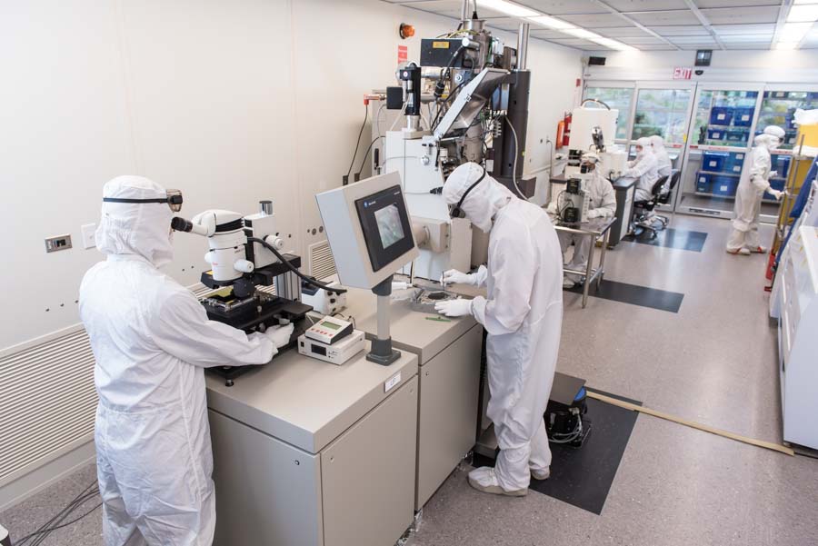
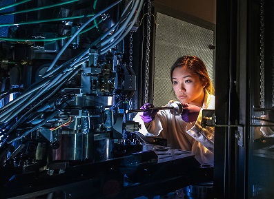
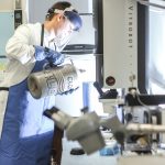
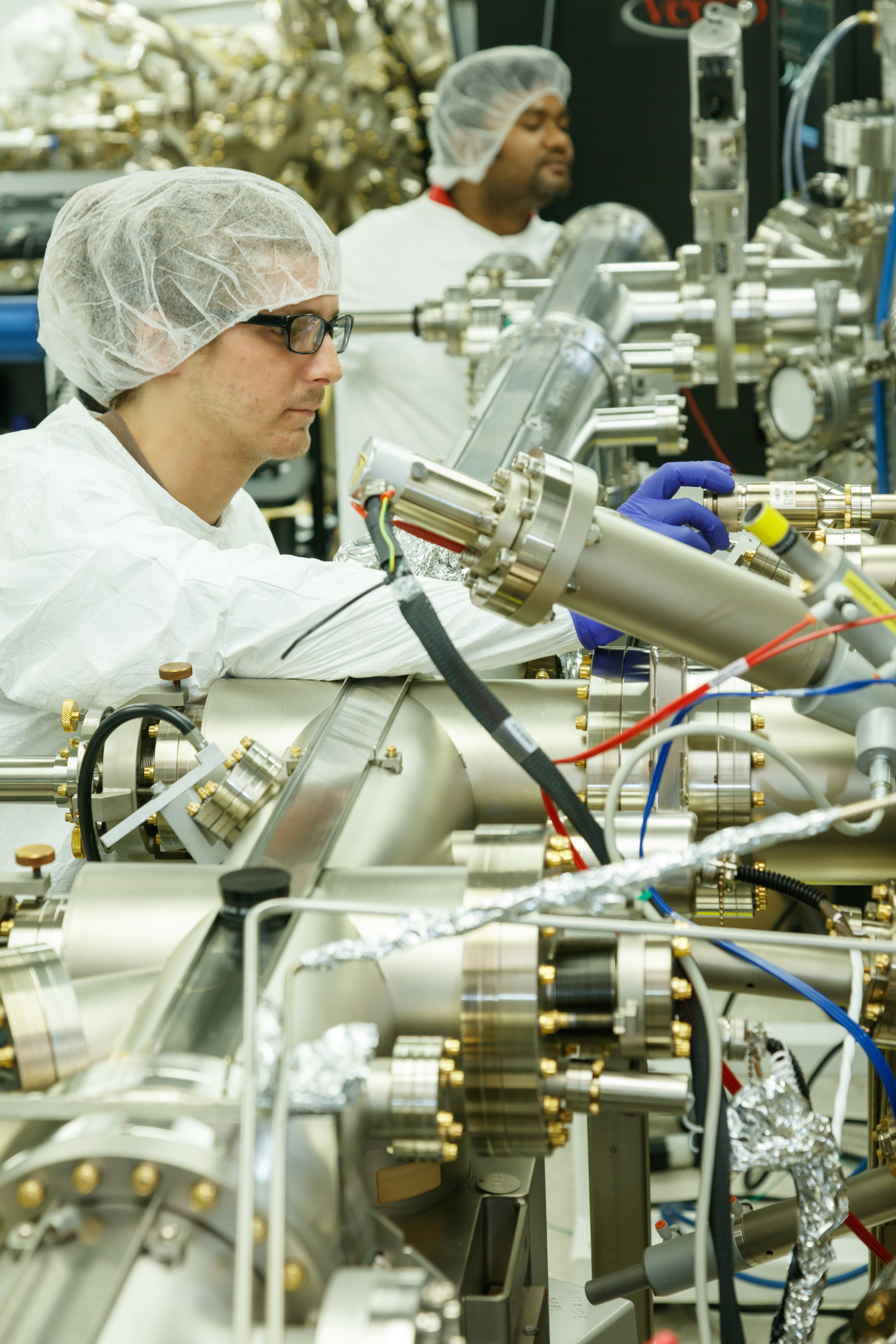
 Nanotech West Laboratory is the largest and most comprehensive micro‐ and nanofabrication user facility in the state of Ohio. Open to both academic and industrial users, Nanotech West houses a 6,000 square foot class 100 cleanroom with a comprehensive 100mm wafer process flow, a 5,000 square foot Biohybrid Lab, and additional laboratory, administrative, and support space. Home to more than 50 large pieces of user accessible material synthesis, fabrication and metrology equipment, Nanotech West operations are supported by administrative engineering core staff (most with semiconductor industry or manufacturing experience) who provide training, process and project support to Nanotech’s diverse user base. Activities at Nanotech span a range of cutting‐edge materials research that is rather extraordinary for a single facility – from high‐frequency GaN/AlGaN electronics, to solar cells, to microfluidics and biotechnology, to the fabrication of structures for use in the study of basic physics and chemistry. As the primary IMR location on Ohio State’s West Campus, Nanotech West provides substantial impact and continues to be a centerpiece of collaborative research to OSU’s materials research community.
Available Instrumentation
- Electron beam lithography [Vistec® EBPG-5000]
- Metalorganic chemical vapor deposition [Aixtron/Swan® 3˝x 2˝]
- Atomic layer deposition [Picosun® SunALE R-150B]
- Field-emission scanning electron microscopy [Carl Zeiss® Ultra 55 Plus]
- ICP-RIE, inductively coupled plasma reactive ion etching [Plasma-Therm® SLR 770] and several other plasma etch tools
- Wafer bonding and micro– and nanoimprint lithography [EVG 520HE]
- I-V, C-V, L-I-V, microfluidic, and solar device testing
- Atomic force microscopy [Veeco® 3100, NanoInk®, Asylum® BioAFM]
- Full Biohybrid Lab
- Full-flow 100mm process capability including photolithography, wet/dry etching, deposition, oxidation, metrology
- 6,000 square foot class 100 cleanroom
Location: 1305 Kinnear Rd, Suite 100, Columbus, Ohio
Website: http://cemas.osu.edu/
Contact: Hendrik (Henk) Colijn, Associate Director, 614-643-3458, colijn.1@osu.edu
 The Center for Electron Microscopy and Analysis (CEMAS) is the materials characterization hub for business and academia. With one of the largest concentrations of electron and ion beam analytical microscopy instruments in any North American institution, CEMAS brings together multidisciplinary expertise to drive synergy, amplify characterization capabilities, and challenge what is possible in analytical electron microscopy.
 This microscopy facility’s point of difference is their world-class multidisciplinary approach that enables academic and business partners to “see” more than ever before. CEMAS is the center that breaks through the current characterization limitations in medicine, environmental science, energy materials and beyond. The full-service facility – from extensive sample preparation laboratories to post-processing tools and support – allows researchers to carry out their entire microscopy and analysis program at CEMAS. Located in a highly customized facility on The Ohio State University’s West Campus, every instrument in the facility meets or exceeds manufacturer performance specifications. A support team of technical, research, administrative and academic staff based at CEMAS provides comprehensive support to all users through a variety of mechanisms from contract research to collaborative projects.
Ohio State – FEI Electron Microscopy Collaboratory
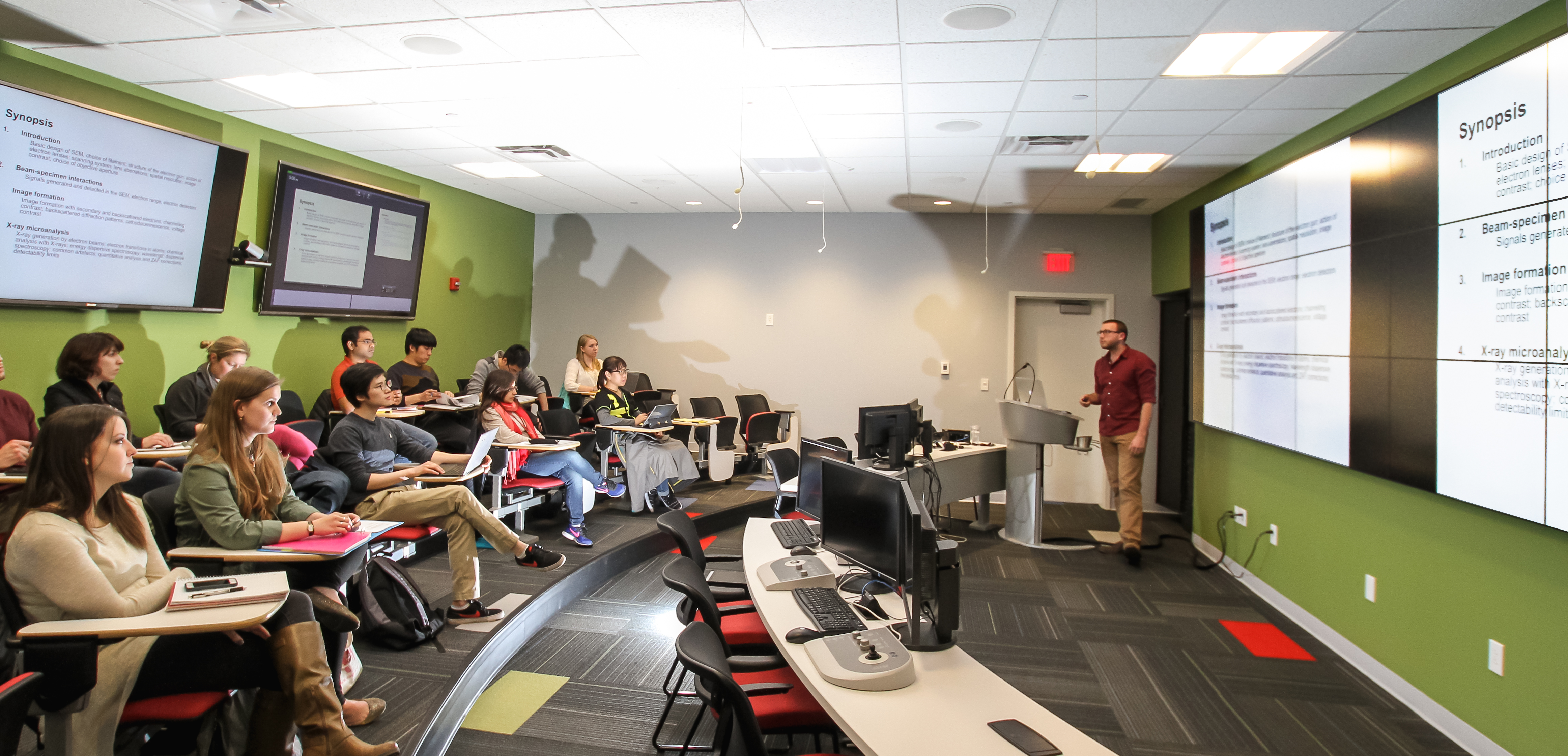 World-class microscopy education in the theory of electron microscopy and all aspects of its use and operation is also available at CEMAS, both in-house and remotely, through our digital theater. Students have live access to CEMAS instruments in real time within a state-of-the-art classroom environment to meet every microscopy training need. Video wall technology provides multiple display screens and projectors, allowing simultaneous display of microscope controls, microscope outputs and lecture slides. Students and lecturers can interact with and operate electron and ion microscopes from within the digital theater in a live, seamless manner – as if one were sitting in front of the instrument. Control of the microscope can be transferred to members of the audience using wired and wireless connectivity.
The microscopes can also be shared with students and researchers at geographically distant locations. Remote operation capabilities connect directly to the 100 Gb/s Ohio OARnet network, providing a unique opportunity for remote teaching and research to partners across the state of Ohio. CEMAS is pioneering the practical application of this technology for research and training of the next generation of electron microscopy specialists, providing an environment to facilitate world-class collaborative research, and maximizing productivity while minimizing economic and environmental impact. This remote electron microscopy collaboratory system has been installed at the University of Dayton, The Ohio State University’s Wooster campus and the Air Force Research Laboratory at Wright-Patterson Air Force Base (Dayton), with additional locations planned for the near future.
Available Instrumentation
- Thermo Scientific Krios
- Thermo Scientific Glacios
- Thermo Scientific Apreo LoVac Analytical
- Thermo Scientific Apreo LoVac High Resolution
- Thermo Scientific Quattro
- Thermo Scientific Themis Z
- FEI Image Corrected Titan 60-300 S/TEM
- FEI Tecnai F20 S/TEM
- FEI Helios NanoLab 600 DualBeam (FIB/SEM)
- FEI Nova NanoLab 600 DualBeam (FIB/SEM)
- FEI Quanta 200 SEM
- Rigaku MiniFlex 600
- Rigaku SmartLab
Website: http://ensl.osu.edu/
Contact: Dr. Denis V. Pelekhov, Lab Manager, pelekhov.1@osu.edu, 614-292-9125
Download the NSL flyer
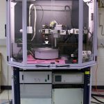 NanoSystems Laboratory (NSL) provides users with access to advanced material characterization and fabrication tools for research and development applications. NSL operates a diverse set of research instrumentation and research capabilities including Focused Ion Beam/Scanning Electron Microscopy, X-ray diffractometry, SQUID magnetometry, Atomic Force/Magnetic Force microscopy, EDS X-ray microanalysis, Langmuir-Blodgett trough monolayer deposition, e-beam lithography, Electron Spin Resonance spectroscopy, Physical Vapor material deposition, ion milling, maskless photo lithography, Low‐Temperature/High Magnetic field magnetotransport measurements, diamond CVD growth, material polishing, Kerr microscopy, THz spectroscopy, critical point drying and magneto-optical material studies. NSL also operates two 1,600 ft2 clean room facilities. One clean room houses instruments for material deposition and photo lithography, while the other clean room is devoted to processing organic spintronics devices, organic photovoltaics, organic LEDs, and other air and moisture sensitive materials. It is equipped with four interconnected gloveboxes with Ar and N2 atmosphere. Equipment installed in the gloveboxes includes an organic deposition chamber, metal deposition chamber, parylene deposition system, a spin coater, a solar simulator, wiring station and a system for electrical testing.
Available Instrumentation
- Focused Ion Beam/Scanning Electron Microscope (FIB/SEM) – FEI Helios Nanolab 600 Dual Beam sophisticated platform for sample preparation, imaging and analysis. High-performance ion column, Platinum deposition, X-ray EDS microanalysis and custom e-beam lithography.
- 2 SQUID Magnetometers – One Quantum Design MPMS system and one MPMS XL system for magnetic sample characterization. A very sensitive tool for measuring DC sample magnetic moment.
- 2 Atomic Force/Magnetic Force Microscopes (AFM/MFM) – One Bruker Dimension Icon and one Dimension 3000 Scanning Probe Microscope.
- Langmuir-Blodgett Trough (LBT) – NIMA Technology model 612D trough used for studying properties of monolayers of amphiphilic molecules and for depositing molecular monolayers on various substrates.
- X-Ray Diffractometer (XRD) – Bruker D8 Discover high-resolution triple-axis X-ray diffractometer with high performance optics for optimum resolution.
- Low-Temperature Magnetotransport Measurement System (LTMT) – Can be used to measure electrical properties of materials and devices at low temperatures and in magnetic field
- Lab-18 Thin Film Deposition system installed in a clean room environment with RF and DC sputtering and e-beam deposition capabilities. Optimized for sputter deposition of magnetic metals and/or oxides followed by coating with a precious metal (gold, platinum, etc.) using e-beam deposition.
- 14 T Physical Properties Measurement System (PPMS) with a cryogenic Atomic Force Microscope/Magnetic Force Microscope (AFM/MFM).
- Diamond Chemical Vapor Deposition System (CVD) for synthesizing high quality poly crystalline and single crystal diamond films for research and production.
- Other available instruments include a Wire Bonder, a Critical Point Dryer, two Terahertz spectrometers, a Magneto-optical Kerr Microscope, and a new optical microscope.
- New instruments available soon include an Electron Paramagnetic Resonance (EPR) spectrometer, and a laser writer for mask-free photo lithography installed in a clean room environment.
Locations:
SEAL Molecular Beam Epitaxy (MBE) Lab (Cleanroom): 095 Dreese Laboratories, 2015 Neil Avenue, Columbus, Ohio
SEAL Analysis Lab: 360 Caldwell Laboratory, 2024 Neil Avenue, Columbus, Ohio
Website: https://seal.osu.edu/
Contact: Mark Brenner, Lab Manager, 614-688-4568, brennerm@ece.osu.edu
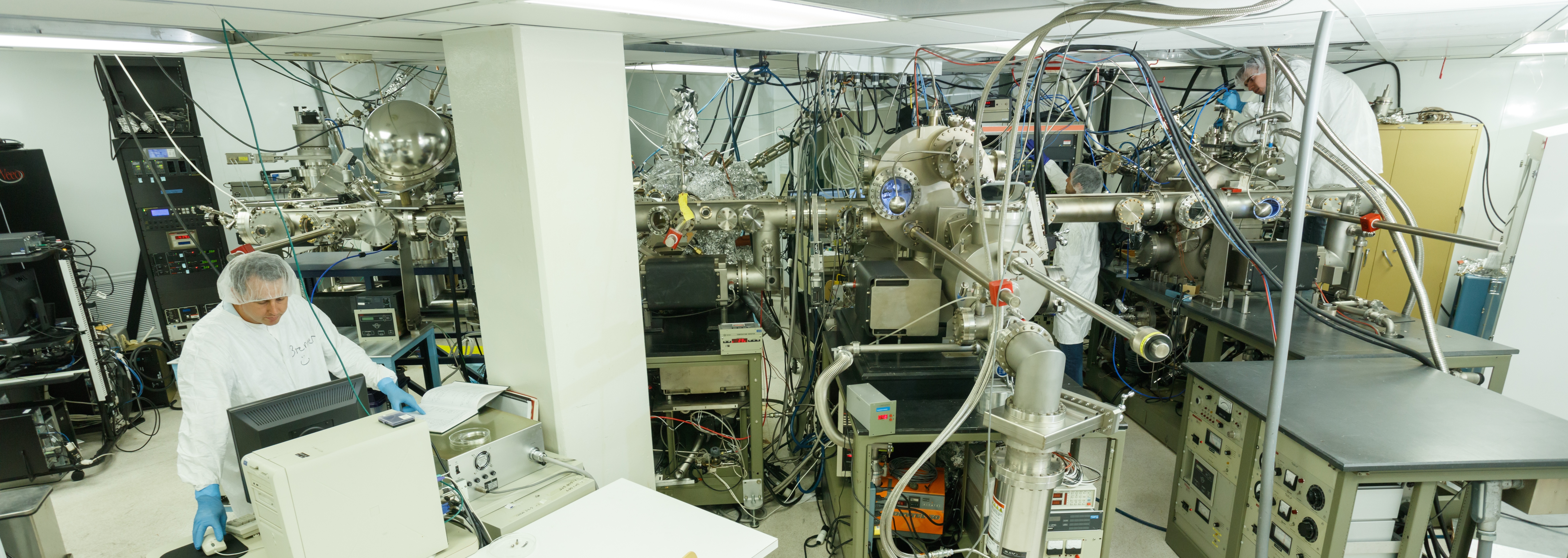
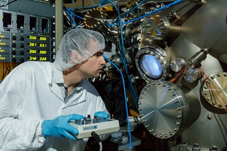 The Semiconductor Epitaxy and Analysis Laboratory (SEAL) is Ohio State’s primary facility for molecular beam epitaxy (MBE). SEAL is home to five state of the art MBE chambers, each dedicated to different, complementary material systems, to ensure high quality material epitaxy for both basic studies and true device development. Research is focused ona broad range of semiconductor materials, including AlGaInAsP, AlGaInNx and SiGe. Several chambers are integrated into ultra-high vacuum (UHV) cluster tools enabling an unusual range of hybrid structures and devices.
Vacuum Cluster I encompasses two MBE chambers and an analytical system allowing III-V/IV integration studies and high resolution x-ray photoelectron spectroscopy (XPS) for in-situ chemical studies of pristine surfaces and interfaces. Vacuum Cluster II enables growth of magnetic epilayers and spin detectors on pristine nitride hetereostructures through two MBE chambers. The lab also includes a wide range of advanced, state of the art materials characterization tools to support advanced epitaxy and forefront advances in electronic materials. SEAL is a fully staffed user facility open to university and industry researchers.
Available Instrumentation
- MBE1: Highly modified 3 inch Varian GENII solid source III-V MBE chamber for GaAlInAsP family of materials
- MBE2: Solid source MBE chamber for epitaxial metals, spintronic metals, Si and Ge.
- MBE3: 3 inch Varian GENII based solid source MBE chamber for exploratory materials (currently under renovation)
- MBE4: Veeco 930 solid source Plasma-assisted MBE chamber for AlGaInN family materials
- MBE5: NH3-based III-N MBE chamber (under construction)
- X-ray photoelectron spectroscopy (XPS) analytic chamber, interconnected with MBE1,2,3 systems; includes monochromatized Al Kα x-ray source and temperature-dependent measurements
- BEDE D1 High Resolution Triple Axis X-ray Diffraction System with x-ray reflectivity, symmetric and assymetric reciprocal space mapping, environmental stage and x-ray topography
- Variable field and temperauture Lakeshore Cryotronics Hall Effect system, including QMSA capability; temperature range is 10k-325K and with fields up to 10T
- Photoluminescence (PL) Spectroscopy: Low temperature capability and 488nm Argon laser
Other Facilities
The Ohio State University is also home to several other materials-related instrumentation centers, facilities, and laboratories on campus. All of these facilities are available to researchers within the Ohio State materials community and to external users. For more information on those facilities, visit their websites linked below:
- Analytical Spectroscopy Laboratory
- Campus Chemical Instrumentation Center (CCIC)
- Campus Microscopy and Imaging Facility (CMIF)
- Center for Chemical and Biophysical Dynamics (CCBD)
- Electronic Materials and Nanostructures Laboratory (EMNLAB)
- Mass Spectrometry and Proteomics Facility
- Microelectronics Laboratory
- Nanoprobe Laboratory for Bio- & Nanotechnology and Biomimetics (NLBB)
- Nuclear Magnetic Resonance Laboratory
- Surface Analysis Facility
- Trace Element Research Laboratory (TERL)
- X-ray Crystallography Laboratory